

Semiconductor device and manufacturing method thereof
a semiconductor and semiconductor technology, applied in semiconductor devices, semiconductor/solid-state device details, electrical apparatus, etc., can solve the problems of metal diffusion contaminating the first wafer, the limitation of the tsv nested hole structure in practical applications, etc., to improve the adhesion, good surface coverage, and good compactness
- Summary
- Abstract
- Description
- Claims
- Application Information
AI Technical Summary
Benefits of technology
Problems solved by technology
Method used
Image

Examples
Embodiment Construction
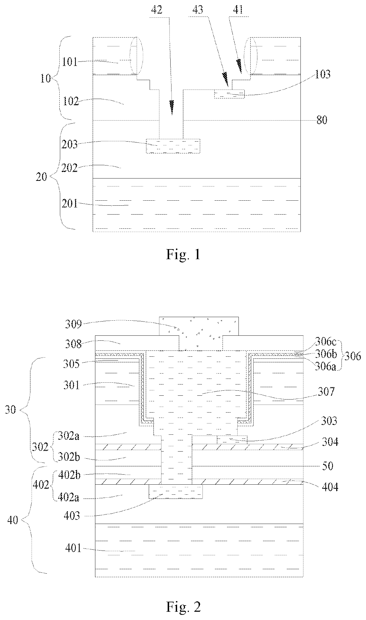
[0067]As described in the background, the TSV nested hole structure can largely satisfy the requirements of the metal interconnection after bonding. However, the inventors have found that the current TSV nested hole structure has limitations in realizing metal interconnection in practical applications. The reason is that in the process of performing dry etching to expose the first metal layer and the second metal layer, if a certain degree of over-etching is not performed, the first metal layer and the second metal layer are easily exposed insufficiently, but if over-etching is performed, it is easy for metal to be splashed back to the first substrate, thereby causing metal diffusion to contaminate the first wafer.
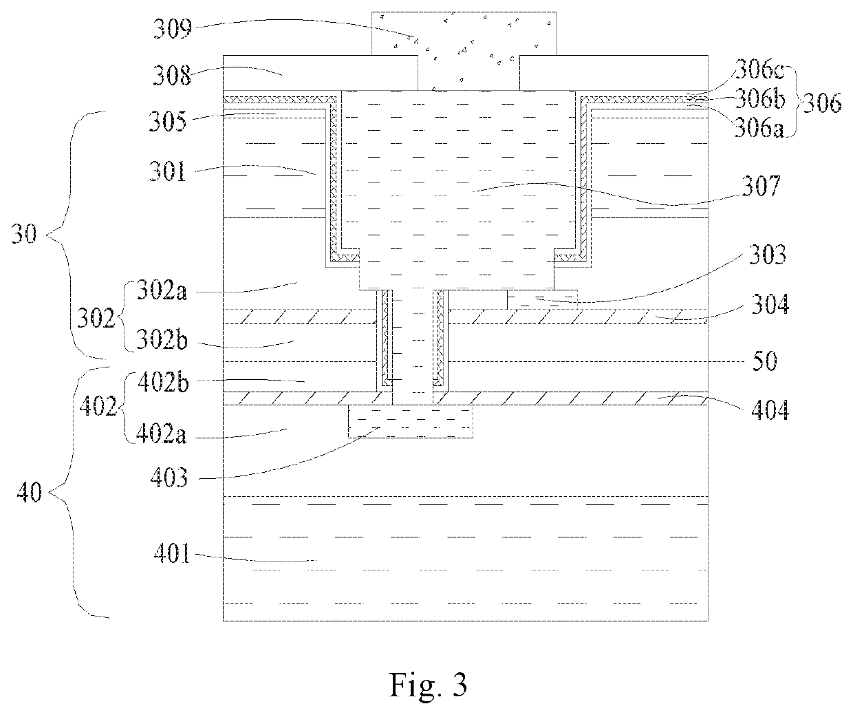
[0068]Specifically, as shown in FIG. 1, the first wafer 10 and the second wafer 20 are bonded to each other. The first wafer 10 includes a first substrate 101, a first dielectric layer 102 located on the first substrate 101 and a first metal layer 103 embedded in the first...
PUM
| Property | Measurement | Unit |
|---|---|---|
| width | aaaaa | aaaaa |
| dielectric | aaaaa | aaaaa |
| cross section width | aaaaa | aaaaa |
Abstract
Description
Claims
Application Information