Heat treatment method for managing dummy wafer

a treatment method and dummy wafer technology, applied in ohmic-resistance heating, electrical apparatus, ohmic-resistance heating devices, etc., can solve problems such as contamination in the chamber, cracking and warpage prone to occur in the dummy wafer, and temperature history differences

Active Publication Date: 2021-06-01
DAINIPPON SCREEN MTG CO LTD
View PDF19 Cites 0 Cited by
  • Summary
  • Abstract
  • Description
  • Claims
  • Application Information

AI Technical Summary

Benefits of technology

[0015]The method is capable of appropriately managing the deterioration of dummy wafers to reliably grasp a dummy wafer suffering advanced deterioration.

Problems solved by technology

Unfortunately, the temperature of in-chamber structures (structures in a chamber including a susceptor for holding a semiconductor wafer and the like changes in some cases in the course of the sequential processing or treatment of semiconductor wafers in a lot.
Changes in temperature of the in-chamber structures including the susceptor and the like in the course of the treatment of semiconductor wafers in a lot give rise to a problem that there arises a difference in temperature history during the treatment between initial semiconductor wafers and latter semiconductor wafers in the lot.
As a result, deterioration of the dummy wafers proceeds to accordingly make cracking and warpage prone to occur in the dummy wafers.
The occurrence of cracking and warpage in the dummy wafers during the dummy running causes contamination in the chamber and transport trouble.
In conventional techniques, however, the deterioration condition has not sufficiently been grasped because an operator views or writes on paper the treatment history of the dummy wafers to manage the treatment history.
This has resulted in a problem that heating treatment is accidentally performed on a dummy wafer suffering excessively advanced deterioration.

Method used


Image

  • Heat treatment method for managing dummy wafer
  • Heat treatment method for managing dummy wafer
  • Heat treatment method for managing dummy wafer

Examples


first preferred embodiment

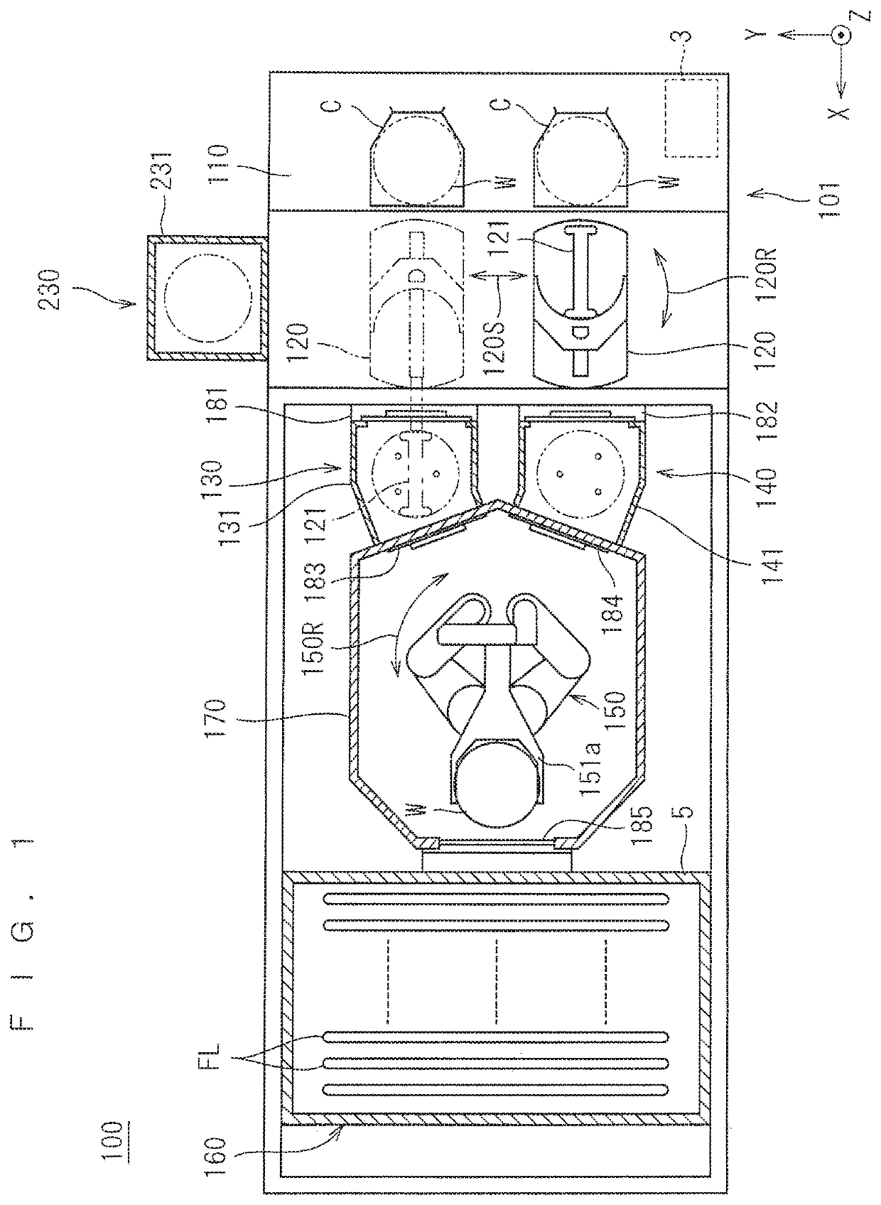
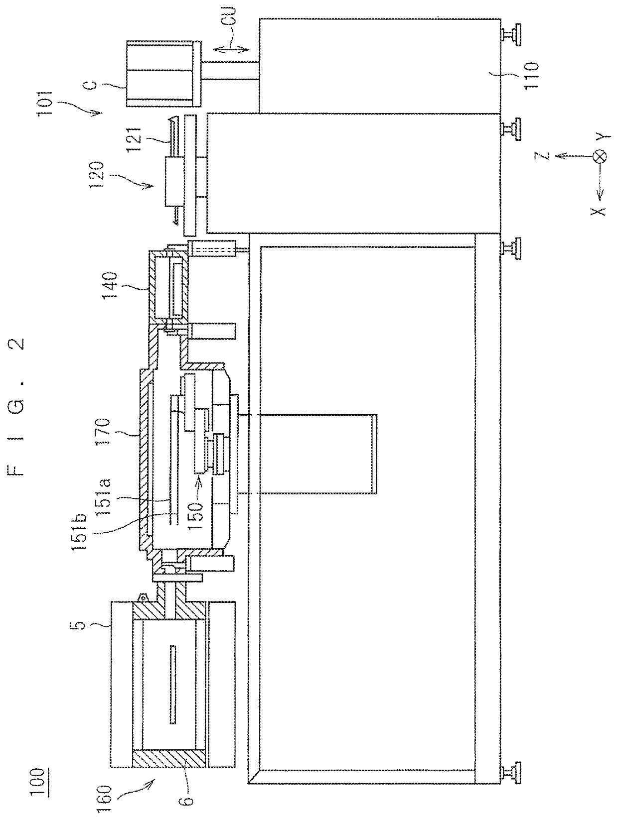
[0031]First, a heat treatment apparatus according to the present invention will be described. FIG. 1 is a plan view of a heat treatment apparatus 100 according to the present invention, and FIG. 2 is a front view of the heat treatment apparatus 100. The heat treatment apparatus 100 is a flash lamp annealer for irradiating a disk-shaped semiconductor wafer W serving as a substrate with flashes of light to heat the semiconductor wafer W. The size of the semiconductor wafer W to be treated is not particularly limited. For example, the semiconductor wafer W to be treated has a diameter of 300 mm and 450 mm. The semiconductor wafer W prior to the transport into the heat treat me apparatus 100 is implanted with impurities. The heat treatment apparatus 100 performs heating treatment on the semiconductor wafer W to thereby activate the impurities implanted in the semiconductor wafer W. It should be noted that the dimensions of components and the number of components are shown in exaggeratio...

second preferred embodiment

[0115]Next, a second preferred embodiment according to the present invention will be described. The second preferred embodiment is similar in configuration of the heat treatment apparatus 100 and in procedure for treatment of the semiconductor wafer W to the first preferred embodiment. The second preferred embodiment is substantially similar in details of the management of the dummy wafer (FIG. 11) to the first preferred embodiment. The second preferred embodiment is different from the first preferred embodiment in details of the wear-and-tear value indicating the degree of deterioration of the dummy wafer.

[0116]In the second preferred embodiment, the calculation part 31 calculates an input electric power counter as the wear-and-tear value. The input electric power counter is calculated by adding up the amounts of electric power inputted to the halogen lamps HL which are measured when the dummy wafer is preheated by irradiation with light from the halogen lamps HL. Specifically, the...

third preferred embodiment

[0119]Next, a third preferred embodiment according to the present invention will be described. The third preferred embodiment is similar in configuration of the heat treatment apparatus 100 and in procedure for treatment of the semiconductor wafer W to the first preferred embodiment. The third preferred embodiment is substantially similar in details of the management of the dummy wafer (FIG. 11) to the first preferred embodiment. The third preferred embodiment is different from the first preferred embodiment in details of the wear-and-tear value indicating the degree of deterioration of the dummy wafer.

[0120]In the third preferred embodiment, the calculation part 31 calculates a discharge voltage counter as the wear-and-tear value. The discharge voltage counter is calculated by adding up the discharge voltages of the flash lamps FL measured when the dummy wafer is flash heated by irradiation with flashes of light from the flash lamps FL. Electric power is supplied from high-capacita...


PUM


Abstract

Dummy running is carried out which performs preheating treatment using halogen lamps and flash heating treatment using flash lamps on a dummy wafer to control the temperature of in-chamber structures including a susceptor and the like. In this process, a wear-and-tear value is calculated by adding up the amounts of electric power inputted to the halogen lamps or the like each time the preheating treatment or the flash heating treatment is performed. The wear-and-tear value is an indicator indicating the degree of deterioration of the dummy wafer. If the wear-and-tear value of the dummy wafer is not less than a predetermined threshold value, an alarm is issued. This allows an operator of a heat treatment apparatus to recognize that the deterioration of the dummy wafer reaches a limit value and to reliably grasp the dummy wafer suffering advanced deterioration.

Description

BACKGROUND OF THE INVENTIONField of the Invention[0001]The present invention relates to a heat treatment method which manages dummy wafers.Description of the Background Art[0002]In the process of manufacturing a semiconductor device, attention has been given to flash lamp annealing (FLA) which heats a semiconductor wafer in an extremely short time. The flash lamp annealing is a heat treatment technique in which xenon flash lamps (the term “flash lamp” as used hereinafter refers to a “xenon flash lamp”) are used to irradiate a surface of a semiconductor wafer with a flash of light, thereby raising the temperature of only the surface of the semiconductor wafer in an extremely short time (several milliseconds or less).[0003]The xenon flash lamps have a spectral distribution of radiation ranging from ultraviolet to near-infrared regions. The wavelength of light emitted from the xenon flash lamps is shorter than that of light emitted from conventional halogen lamps, and approximately coi...

Claims


Application Information

Patent Timeline
Patent Type & Authority Patents(United States)
IPC IPC(8): H01L21/67H01L21/324
CPCH01L21/67098H01L21/324H01L21/67248H01L21/2636H01L21/67115H01L21/67288H01L21/6875H01L21/68707H05B3/0047H05B2203/032
Inventor UENO, TOMOHIROFUSE, KAZUHIKOOMORI, MAO
Owner DAINIPPON SCREEN MTG CO LTD
Why Eureka
Try Eureka