Methods for etching a hardmask layer

a technology of etching process and hardmask layer, which is applied in the direction of electrical equipment, basic electric elements, electric discharge tubes, etc., can solve the problems of limiting the aspect ratio that may be obtained, and the development of etch processes capable of reliably forming features with such high aspect ratios, so as to facilitate the profile and dimension control of features

Active Publication Date: 2021-09-21
APPLIED MATERIALS INC
View PDF25 Cites 0 Cited by
  • Summary
  • Abstract
  • Description
  • Claims
  • Application Information

AI Technical Summary

Benefits of technology

[0009]Methods for etching a hardmask layer to transfer features into a material layer using an etch process are provided. The methods described herein advantageously facilitate profile and dimension control of features through a proper sidewall and bottom management scheme during the hardmask open process. In one embodiment, a method for etching a hardmask layer to form features in the hardmask layer includes supplying an etching gas mixture onto a substrate to etch an exposed portion of a hardmask layer exposed by a patterned photoresist layer disposed on the substrate, switching the etching gas mixture to a deposition gas mixture comprising a silicon containing gas to form a passivation layer on sidewalls of the hardmask layer and forming openings in the hardmask layer.

Problems solved by technology

However, with the continued miniaturization of circuit technology, the dimensions of the size and pitch of circuit features, such as interconnects, have placed additional demands on processing capabilities.
Developing etch processes that are capable of reliably forming features with such high aspect ratios presents a significant challenge.
As the opening of the etched features are narrowed and / or sealed by the accumulated redeposition of material, the reactive etchants are prevented from reaching the lower surface of the features, thus limiting the aspect ratio that may be obtained.
Additionally, as the redeposition material or build-up of by-products may randomly and / or irregularly adhere to the top surface and / or sidewalls of the features being etched, the resulting irregular profile and growth of the redeposition material may alter the flow path of the reactive etchants, thus resulting in bowing or twisting profiles of the features formed in the material layer.
Furthermore, in some cases, after the etching process, the corner features often suffer from rounded top shoulder erosion or undesired non-vertical sidewall etched profile, resulting in critical dimension (CD) loss or deformed profiles.
In accurate profile or structural dimensions may result in collapse of the device structure, eventually leading to device failure and product low yield.
Poor etching selectivity and control occurring during manufacturing processes for such shapes or features in the material layer may undesirably result in an inaccurate profile control, thus eventually leading to device failure.
After a long period of exposure to the aggressive etchants, the hardmask layer as well as the bottom anti-reflective coating (BARC) and / or an anti-reflective coating (ARC) without sufficient etching resistance or sidewall protection may be damaged, resulting in inaccurate pattern transfer and loss of dimensional control.
Thus, during the bottom anti-reflective coating (BARC) and / or an anti-reflective coating (ARC) open process, the occurrence of sidewall profile damage and / or post-etch sidewall roughness in small critical dimension structures pose a significant challenge to structure profile integrity, especially when significant critical dimensions (CD) shrinkage is required during a bottom anti-reflective coating (BARC) and / or an anti-reflective coating (ARC) open process, which may ultimately deteriorate overall device performance.

Method used


Image

  • Methods for etching a hardmask layer
  • Methods for etching a hardmask layer
  • Methods for etching a hardmask layer

Examples


Embodiment Construction

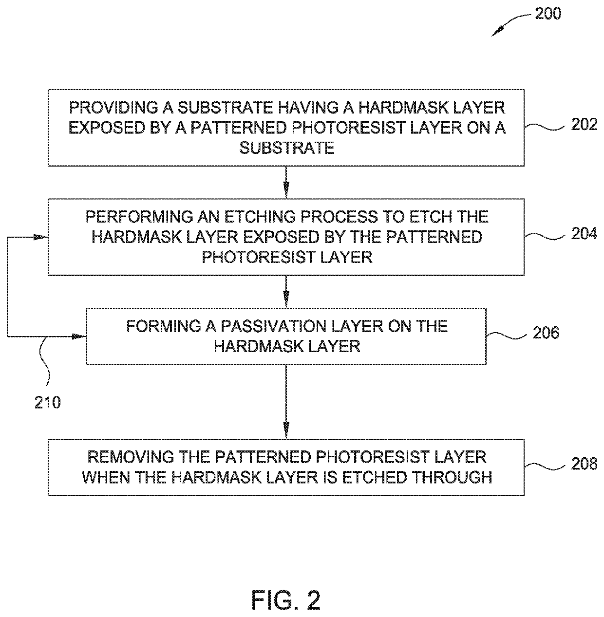
[0018]Embodiments for the present application include methods for etching a hardmask layer to form feature therein. In one embodiment, the method includes plasma etching a hardmask layer using a controlled gas ratio to form a passivation layer while etching the hardmask layer. By utilizing a passivation layer during etching, a sidewall / surface protection mechanism formed during the etching process is used to efficiently control the etching profile while etching the hardmask layer. The good bottom as well as sidewall protection during the etching process enables etching the hardmask layer with a desired profile, thus assisting transferring features with desired profile to the underlying structures / layers while retaining good profile control and critical dimensions.

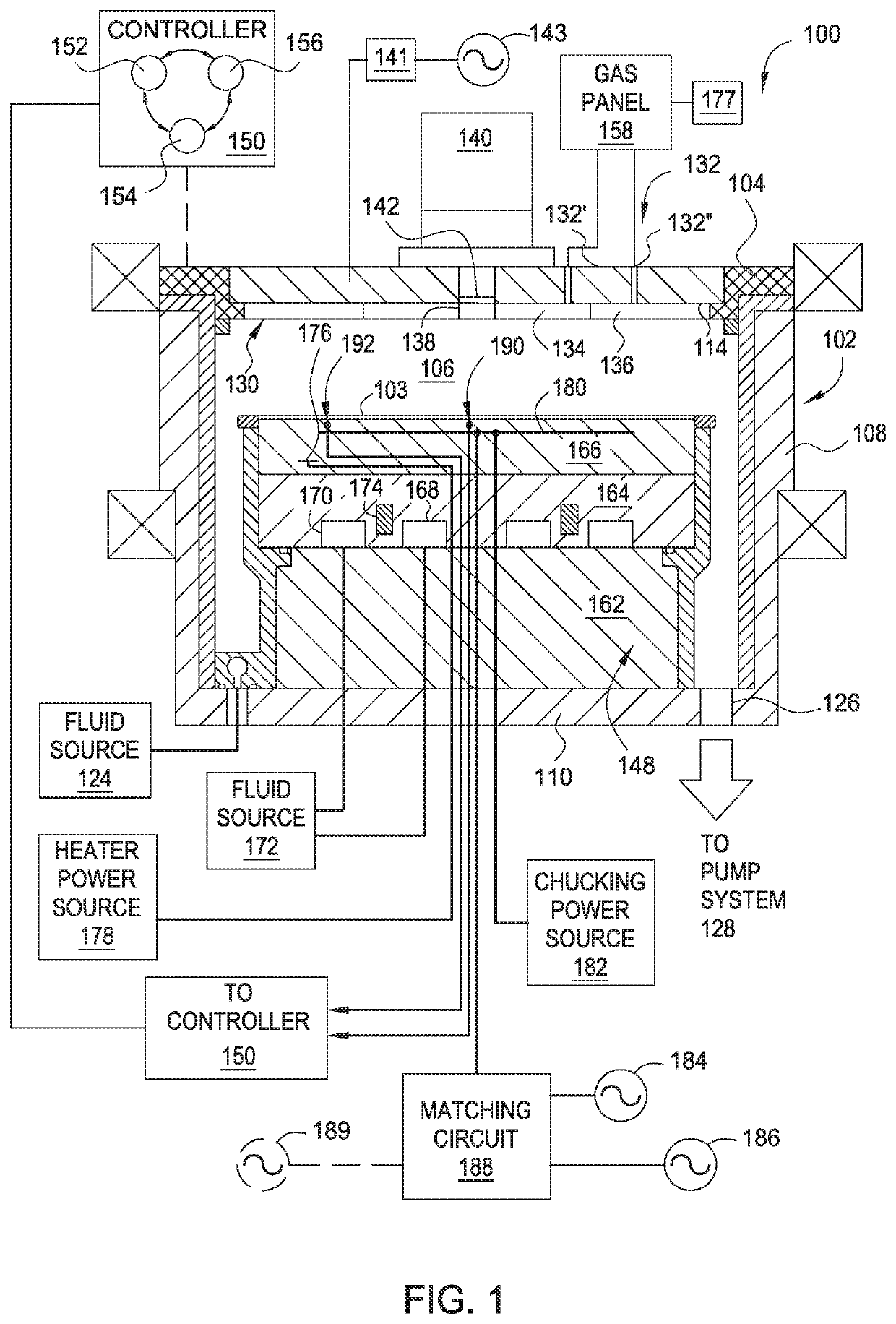
[0019]FIG. 1 is a sectional view of one example of a processing chamber100 suitable for performing a patterning / etching process to etch a hardmask layer on a substrate using an etching process. Suitable processing chambers ...


PUM

PropertyMeasurementUnit
operating pressuresaaaaaaaaaa
frequencyaaaaaaaaaa
diameteraaaaaaaaaa

Abstract

Methods for etching a hardmask layer to transfer features into a material layer using an etch process are provided. The methods described herein advantageously facilitate profile and dimension control of features through a proper sidewall and bottom management scheme during the hardmask open process. In one embodiment, a method for etching a hardmask layer to form features in the hardmask layer includes supplying an etching gas mixture onto a substrate to etch an exposed portion of a hardmask layer exposed by a patterned photoresist layer disposed on the substrate, switching the etching gas mixture to a deposition gas mixture comprising a silicon containing gas to form a passivation layer on sidewalls of the hardmask layer and forming openings in the hardmask layer.

Description

CROSS-REFERENCE TO RELATED APPLICATIONS[0001]This application claims benefit of U.S. Provisional Application Ser. No. 62 / 616,935 filed Jan. 12, 2018, which is incorporated by reference in its entirety.BACKGROUND OF THE DISCLOSUREField[0002]The embodiments herein generally relate to an etching process for etching a hardmask layer, such as a dielectric layer, with high selectivity and good profile control.Description of the Background Art[0003]Reliably producing submicron and smaller features is one of the key requirements of very large scale integration (VLSI) and ultra large scale integration (ULSI) of semiconductor devices. However, with the continued miniaturization of circuit technology, the dimensions of the size and pitch of circuit features, such as interconnects, have placed additional demands on processing capabilities. The multilevel interconnects that lie at the heart of this technology require precise imaging and placement of high aspect ratio features, such as vias and o...

Claims


Application Information

Patent Timeline
Patent Type & Authority Patents(United States)
IPC IPC(8): H01L21/311H01J37/32
CPCH01L21/31122H01J37/32522H01J37/32724H01L21/31144
Inventor JIANG, SHANLEE, GENEMEHROTRA, AKHILHESABI, ZOHREH
Owner APPLIED MATERIALS INC
Why Eureka
Try Eureka