Method for producing a component by filling a cavity within an electrical isolation area with carbon-based material

a carbon-based material and cavity filling technology, applied in the direction of basic electric elements, electrical equipment, semiconductor devices, etc., can solve the problems of short circuit of neighbouring microelectronic components, damage to the integrity of dielectric materials, and residual voids that cannot be filled by other layers

Active Publication Date: 2022-07-12
COMMISSARIAT A LENERGIE ATOMIQUE ET AUX ENERGIES ALTERNATIVES
View PDF8 Cites 0 Cited by
  • Summary
  • Abstract
  • Description
  • Claims
  • Application Information

AI Technical Summary

Benefits of technology

[0024]The present invention thus provides a solution allowing to stop a deepening of the cavities present in the electrical isolation areas (isolation trenches) after forming the spacers of the transistors. This solution optionally allows to eliminate these cavities by filling them with the filling material. Although it is advantageous that the cavities are completely removed, by a complete filling of their volume, it is possible to operate only a partial filling which, at the very least, limits the disadvantages of the cavities. Optionally, this partial filling can line the wall of the cavity to form a layer which is more resistant to the treatment steps to be followed (including etchings) than the layer wherein the cavities are present.
[0026]The gradual consumption of the material of the isolation trenches during these various subsequent steps is thus prevented. The size of the cavities remains limited. This allows to prevent the formation of residual voids after depositing the stress liner.
[0031]The filling by the stress liner of the spaces between the gates is improved. Residual voids are avoided.

Problems solved by technology

But their deposition causes filling defects which result in the short-circuiting of neighbouring microelectronic components.
Note that these steps generally include one or more heat treatments as well as (wet and / or plasma) cleaning phases which are also damaging to the integrity of the dielectric material.
Unfortunately, these residual voids cannot be filled by other layers above the mechanically constraining layer 15, such as a top electrical isolation layer generally made of silicon dioxide.
This can have adverse consequences when one of these voids is opened during subsequent formation of electrical contacts, in particular when a problem with the alignment of these contacts occurs.
The size of the cavities remains limited.

Method used


Image

  • Method for producing a component by filling a cavity within an electrical isolation area with carbon-based material
  • Method for producing a component by filling a cavity within an electrical isolation area with carbon-based material
  • Method for producing a component by filling a cavity within an electrical isolation area with carbon-based material

Examples


first embodiment

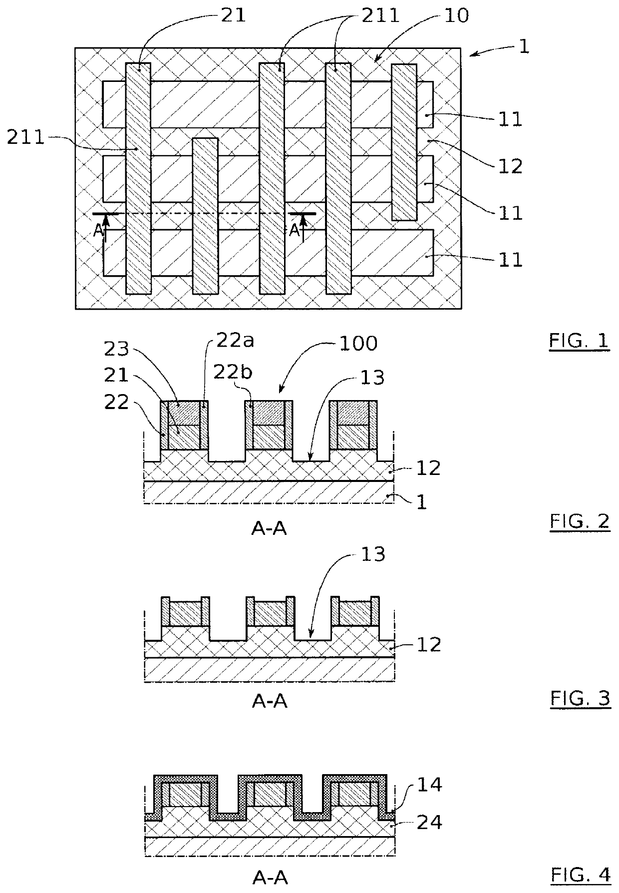
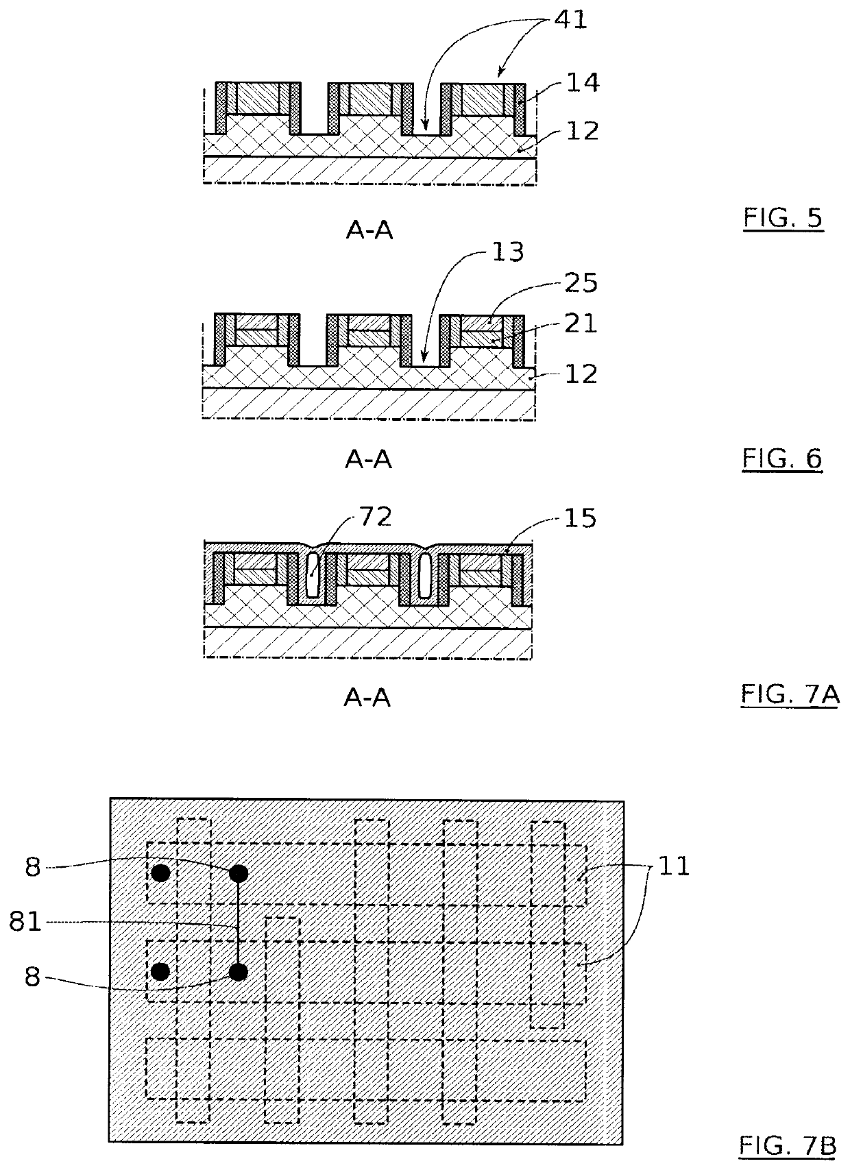
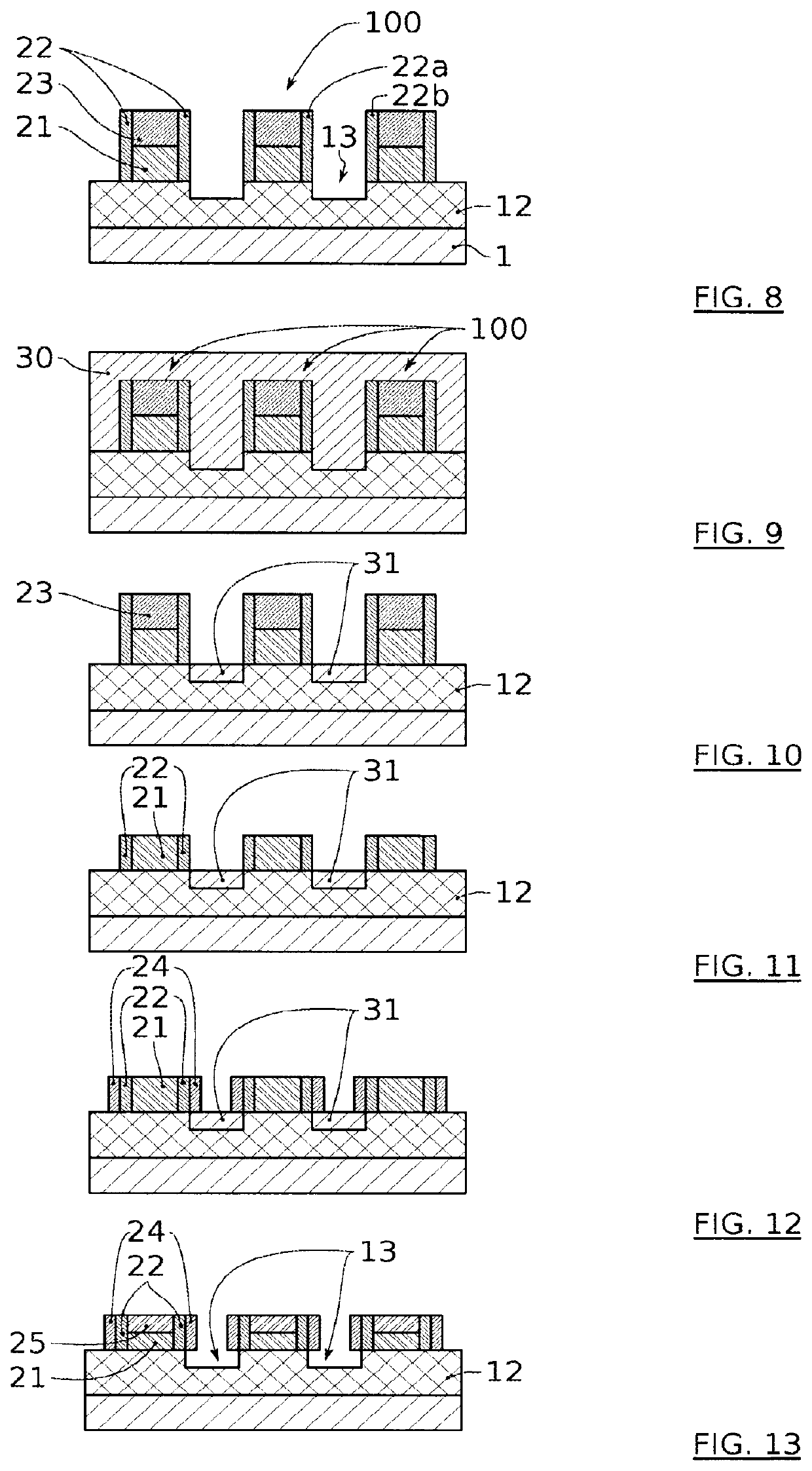
[0112] illustrated in FIGS. 8 to 13, the method comprises, after forming the first spacers 22 and after a first doping by implantation, a step of filling the cavities by depositing a carbon material.

[0113]As illustrated in FIG. 9, a deposition of a carbon layer 30 can be carried out for example by centrifugation, so as to fill the spaces between the gate patterns 100. This carbon layer 30 can optionally cover the top of the gate patterns 100. This layer 30 can thus be used to encapsulate all the underlying elements.

[0114]This carbon layer 30, for example amorphous carbon, can be, without limitation, formed from a carbon resin whose viscosity properties are adapted to a spreading by centrifugation. Annealing after spreading can allow to evaporate the solvents and / or to crosslink the resin so as to obtain the solid carbon layer 30.

[0115]Various carbon resins can be used, such as: polymethyl methacrylate (PMMA) or polydimethylsiloxane (PDMS).

[0116]The thickness of the carbon layer 30 o...

second embodiment

[0140] illustrated in FIGS. 14 to 17, the method comprises, after forming the spacers and doping by implantation (FIG. 14), a step of filling the cavities by depositing a silicon oxide. More generally, it can be an identical material to the underlying one (the one wherein the STI is formed). This is a material capable of being consumed during at least one of the treatment steps indicated, in particular the etchings, this consumption being advantageously equivalent to that of the STI material.

[0141]As illustrated in FIG. 15, a deposition of a silicon oxide layer 40 is carried out so as to fill the spaces between gate patterns 1. Optionally, the layer 40 may cover the gate patterns so that it forms an encapsulation of all the underlying elements.

[0142]This deposition can be done by one of the following techniques: chemical vapour deposition FCVD (acronym for Furnace Chemical Vapour Deposition), oxide deposition under HARP (acronym for High Aspect Ratio Process) type conditions, Flowab...


PUM

PropertyMeasurementUnit
thicknessaaaaaaaaaa
dielectric constantaaaaaaaaaa
angleaaaaaaaaaa

Abstract

A method is provided for producing a component based on a plurality of transistors on a substrate including an active area and an electrical isolation area, each transistor including a gate and spacers on either side of the gate, the electrical isolation area including at least one cavity formed as a hollow between a spacer of a first transistor of the plurality of transistors and a spacer of a second transistor of the plurality of transistors, the first and the second transistors being adjacent, the method including: forming the gates of the transistors; forming the spacers; and forming a mechanically constraining layer for the transistors; and after forming the spacers and before forming the mechanically constraining layer, forming a filling configured to at least partially fill, with a filling material, the at least one cavity within the electrical isolation area, between the spacers of the first and the second transistors.

Description

TECHNICAL FIELD[0001]The present invention relates to the field of manufacturing microelectronic components. It will find an advantageous but non-limiting application in the manufacture of components based on transistors, these components allowing, for example, to form CMOS (for Complementary Metal Oxide Semiconductor) circuits or volatile memories such as Flash memories or non-volatile memories such as SRAM (Static Random Access Memory) memories.PRIOR ART[0002]In the field considered above, technologies are known for manufacturing transistors based on substrates of various technologies. They may be SOI (acronym for Silicon On Insulator) type substrates comprising an underlying semiconductor layer (often silicon), surmounted with an oxide layer called BOX, then a surface semiconductor layer, such as monocrystalline silicon. A refinement of SOI substrates is FDSOI (Fully Depleted Silicon On Insulator) technology, which corresponds to a support of the surface layer type of a fully dep...

Claims


Application Information

Patent Timeline
Patent Type & Authority Patents(United States)
IPC IPC(8): H01L21/8234H01L21/762H01L29/78H01L29/66H01L21/28
CPCH01L21/823481H01L21/28123H01L21/76224H01L21/823468H01L29/6656H01L29/7843H01L21/823418
Inventor POSSEME, NICOLASLE ROYER, CYRILLENEMOUCHI, FABRICE
Owner COMMISSARIAT A LENERGIE ATOMIQUE ET AUX ENERGIES ALTERNATIVES
Why Eureka
Try Eureka