
Wafer acceptance test module and method for a static memory function test

a static memory function and acceptance test technology, applied in the field of semiconductor integrated circuit manufacturing, can solve the problems of inability of the wat test equipment to perform ac tests, measure the dc characteristics of the device, and lack of suitable process development kits (pdks) for chip sram designs

Active Publication Date: 2022-10-04
SHANGHAI HUALI INTEGRATED CIRCUIT CORP
View PDF19 Cites 0 Cited by
  • Summary
  • Abstract
  • Description
  • Claims
  • Application Information

AI Technical Summary

Benefits of technology

The present disclosure describes a wafer acceptance test module for a static memory function test that does not require a dedicated test machine, simplifies the test procedure, achieves simple and robust testing, reduces test equipment costs, and improves test efficiency. This is achieved by providing a reduced instruction built-in self-test circuit consisting of test patterns on the wafer, which enables testing of the static memory using existing wafer acceptance test equipment that can only provide DC voltage, without reliance on a dedicated test machine for memories.

Problems solved by technology

In the prior art, WAT test equipment cannot perform AC tests, and can only measure DC characteristics of devices.
A suitable Process Development Kit (PDK) for chip SRAM designs is lack.
Even if the above problems can be overcome, we only want to perform simple verification, but a relatively large area is needed.
Additional chip designs, hardware, test costs and resources are required.
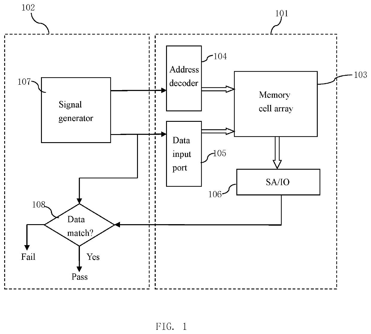
It can be known from the above that the existing method needs to use the ATE equipment 102 to realize the function test of the static memory, the equipment cost is high, and the test procedure is complicated.

Method used


Image

  • Wafer acceptance test module and method for a static memory function test
  • Wafer acceptance test module and method for a static memory function test
  • Wafer acceptance test module and method for a static memory function test

Examples


Embodiment Construction

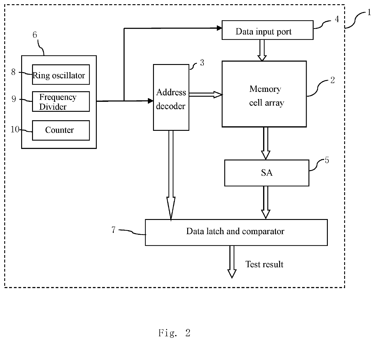
[0046]As shown in FIG. 2, it is a structural diagram of a wafer acceptance test module for a static memory function test according to an embodiment of the present disclosure; the wafer acceptance test module for a static memory function test according to an embodiment of the present disclosure includes a reduced instruction built-in self-test circuit formed on a wafer 1 and consisting of test patterns, and the reduced instruction built-in self-test circuit is for performing a function test for a static memory formed on the wafer 1.

[0047]The static memory includes a memory cell array 2, an address decoder 3, a data input port 4, and a sense amplifier 5.

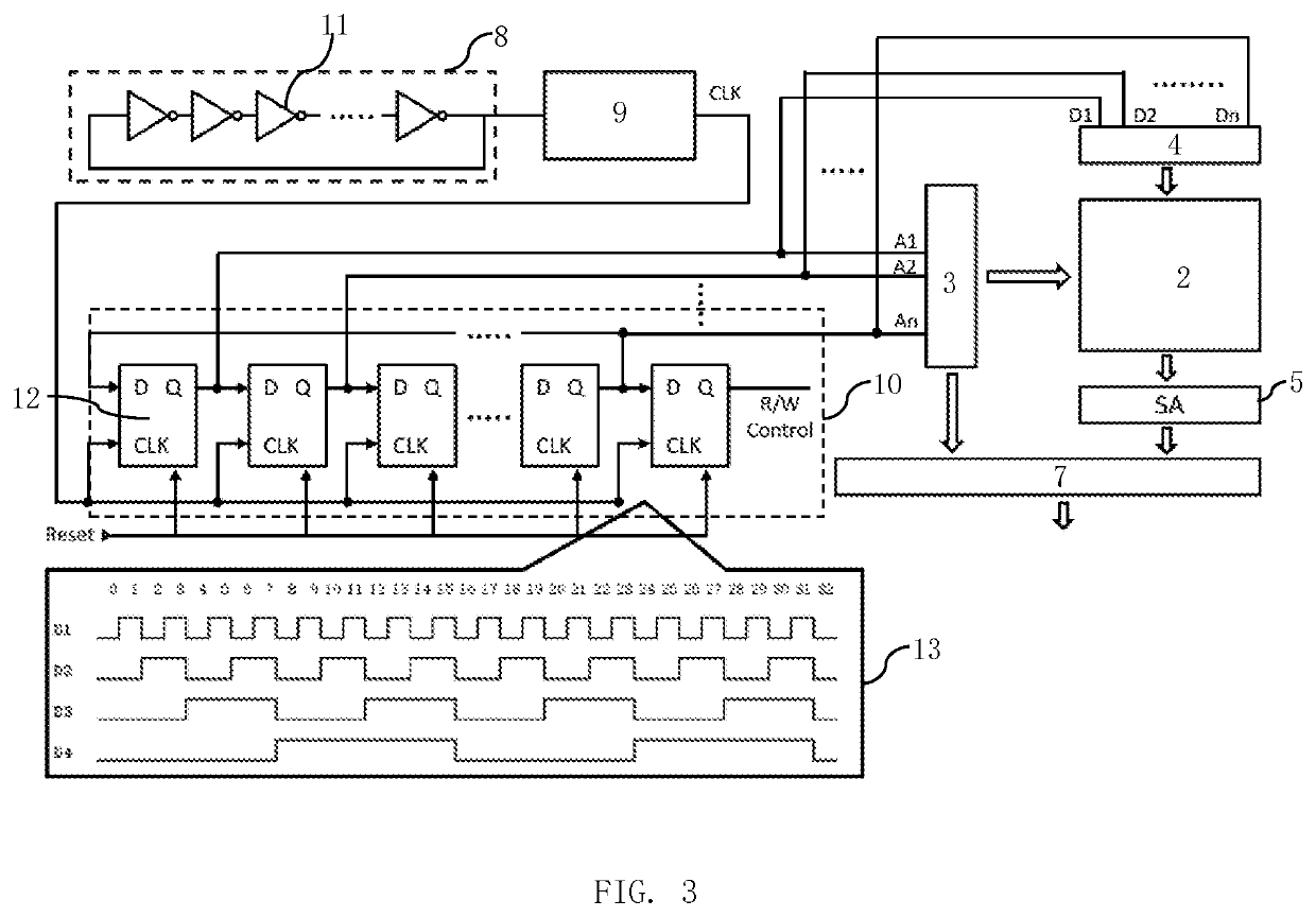
[0048]The reduced instruction built-in self-test circuit includes a ring oscillator 8, a frequency divider 9, a counter 10, and a data latch and comparator 7, wherein the circuit structure consisting of the ring oscillator 8, the frequency divider 9 and the counter 10 is indicated by the reference numeral 6 alone.

[0049]The reduced inst...


PUM


Abstract

The disclosure discloses a wafer acceptance test module for a static memory function test, reduced instruction built-in self-test circuit formed on a wafer includes: a ring oscillator, a frequency divider, a counter, a data latch and comparator. The counter is used for count, and the count is used as an input signal of each of an address decoder and a data input port at the same time. The data latch and comparator is connected to an output terminal of the address decoder and an output terminal of the sense amplifier and compare two output signals to obtain a test result. The disclosure also discloses a wafer acceptance test method for a static memory function test. The disclosure does not need to rely on a dedicated test machine for memory to perform a static memory function test, which can simplify a test procedure.

Description

CROSS REFERENCE TO RELATED APPLICATIONS[0001]The present application claims priority to and the benefit of Chinese Patent Application No. CN 201911052361.X filed on Oct. 31, 2019, the disclosure of which is incorporated herein by reference in its entirety as part of the present application.TECHNICAL FIELD[0002]The disclosure relates to the field of semiconductor integrated circuit manufacturing, in particular to a wafer acceptance test (WAT) module for a static memory function test. The disclosure also relates to a wafer acceptance test method for a static memory function test.BACKGROUND[0003]In the prior art, WAT test equipment cannot perform AC tests, and can only measure DC characteristics of devices. Therefore, functional tests of memories such as the static memory (SRAM) must be performed on custom-designed chips, and can be started until process development is reached to a certain stage. The reasons are as follows.[0004]A suitable Process Development Kit (PDK) for chip SRAM de...

Claims


Application Information

Patent Timeline
Patent Type & Authority Patents(United States)
IPC IPC(8): G11C29/00G11C29/38G11C11/418G11C11/419H03K3/03
CPCG11C29/38G11C11/418G11C11/419H03K3/0315G11C29/56G11C29/56008G11C29/44G11C29/006G11C29/12015H03K5/19
Inventor LAI, ZHENANCHEN, JUNSHENGHUANG, ZHAOYING
Owner SHANGHAI HUALI INTEGRATED CIRCUIT CORP
Learn More