Bulk single crystal gallium nitride and method of making same

a gallium nitride and single crystal technology, applied in envelope/bag making machinery, paper/cardboard containers, applications, etc., can solve the problems of difficult single crystal growth of alloys, difficult production of gan, and difficulty in growing high-quality bulk single crystals, and achieve the effect of improving the final product properties

Inactive Publication Date: 2001-07-19
ADVANCED TECH MATERIALS INC
View PDF0 Cites 125 Cited by
  • Summary
  • Abstract
  • Description
  • Claims
  • Application Information

AI Technical Summary

Benefits of technology

[0021] The layer of single crystal M*N may be deposited directly on the surface of the crystalline or non-crystalline substrate, or alternatively it may be deposited on an uppermost surface of one or more intermediate layers which in turn are deposited on the crystalline substrate. The one or more intermediate layers may serve as a buffer layer to enhance the crystallinity or other characteristics of the M*N layer, as a template for the subsequent M*N growth thereon, or the intermediate layer(s) may serve as protective layer(s), or as an etch stop to prevent the etchant for the sacrificial substrate from etching into the M*N material.
[0024] In another aspect, the invention utilizes the outdiffusion of specific species from the substrate into the M*N layer to provide enhanced properties of the final M*N product. An example of this aspect is the growth of M*N on a silicon substrate. In this case, Si can be caused to diffuse out of the silicon substrate and into the M*N. This diffusion will form a thin M*N region which is heavily doped with silicon. Silicon-doped M*N is n-type, and this structure is advantageous in certain device structures, as for example for making ohmic contacts to the back surface of the M*N layer or for forming p-n junctions.

Problems solved by technology

Such alloys have in the past been difficult to grow in single crystal form.
Unfortunately, however, it heretofore has not been possible to produce GaN in single crystal bulk form, and for all M*N materials, growth of high quality bulk single crystals has been fraught with difficulty.

Method used


Image

  • Bulk single crystal gallium nitride and method of making same
  • Bulk single crystal gallium nitride and method of making same

Examples


Embodiment Construction

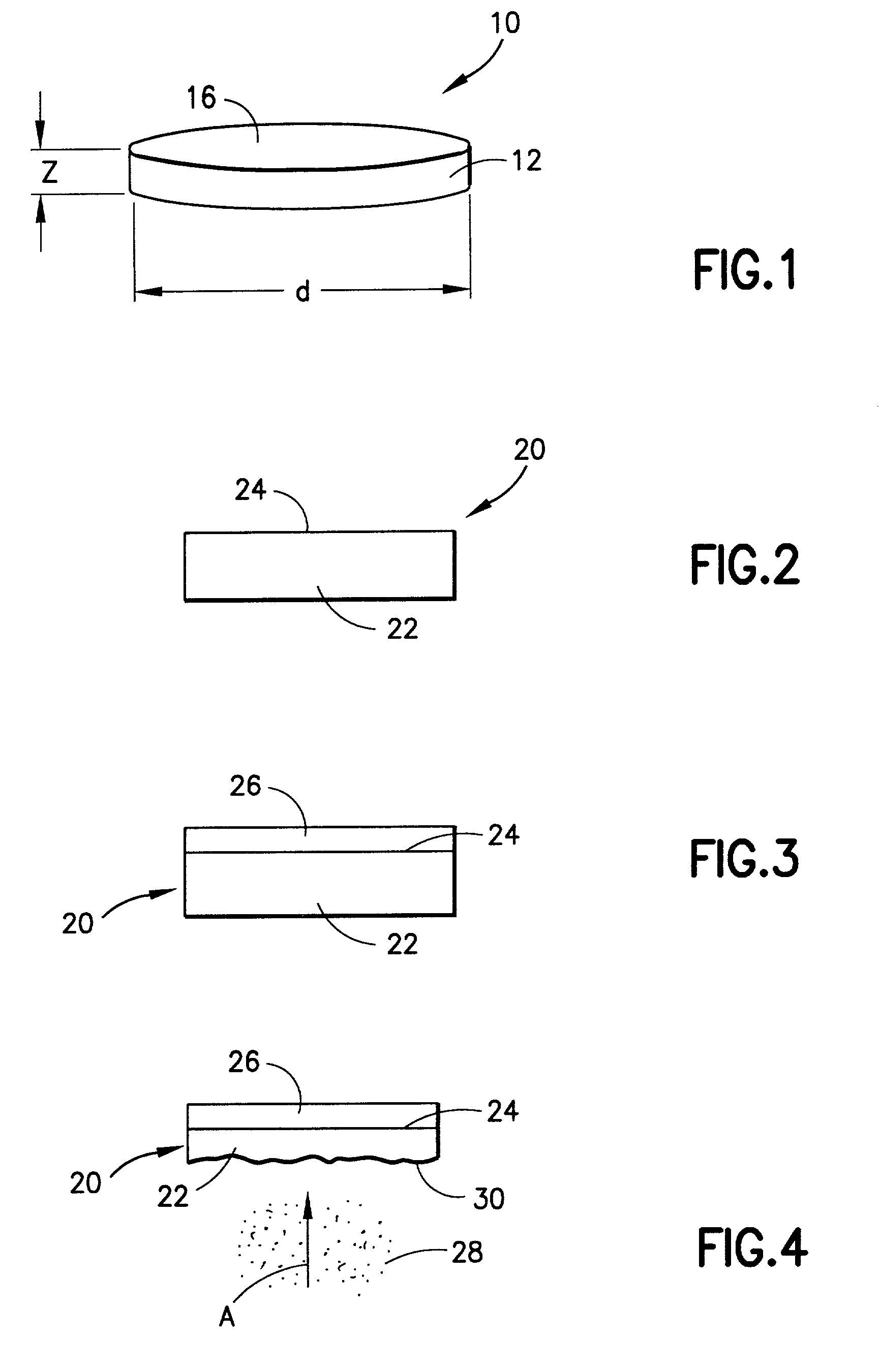
[0037] The present invention is based on the discovery that single crystal M*N articles of a self-supporting structural character can be readily formed by the deposition of single crystal M*N on a substrate epitaxially compatible with the single crystal M*N, followed by in-situ removal of the sacrificial substrate at the growth temperature. The substrate is removed by etching it away from the single crystal M*N, at the M*N growth temperature or at a temperature in proximity to the growth temperature, to yield the single crystal M*N as a product article.

[0038] Since no M*N substrates currently (before the making of the present invention) exist, growth of these compounds must initially take place heteroepitaxially, for example GaN on silicon. Two types of defects arise as a result of heteroepitaxial growth. The first is dislocations due to the lattice mismatch between the M*N layer and the substrate. The typical substrate for GaN is sapphire, which has a 13.8% lattice mismatch to GaN....


PUM

PropertyMeasurementUnit
pressureaaaaaaaaaa
temperatureaaaaaaaaaa
thicknessaaaaaaaaaa

Abstract

A single crystal M*N article, which may be made by a process including the steps of: providing a substrate of material having a crystalline surface which is epitaxially compatible with M*N; depositing a layer of single crystal M*N over the surface of the substrate; and removing the substrate from the layer of single crystal M*N, e.g., with an etching agent which is applied to the substrate to remove same, to yield the layer of single crystal M*N as said single crystal M*N article. The bulk single crystal M*N article is suitable for use as a substrate for the fabrication of microelectronic structures thereon, to produce microelectronic devices comprising bulk single crystal M*N substrates, or precursor structures thereof.

Description

[0001] This is a continuation-in-part of U.S. patent application Ser. No. 08 / 188,469 filed Jan. 27, 1994, issued Oct. 21, 1997 as U.S. Pat. No. 5,679,152 for "Method of Making a Single Crystal Ga*N Article."[0002] 1. Field of the Invention[0003] This invention relates to bulk single crystal binary, ternary or quaternary metal nitrides such as gallium nitride, such metal nitrides being referred to broadly hereafter by the symbol M*N, including single crystal M*N substrate articles useful for formation of microelectronic structures thereon, as well as to an appertaining method of forming M*N in single crystal bulk form.[0004] 2. Description of the Related Art[0005] The III-V nitrides, in consequence of their electronic and optical properties and heterostructure character, are highly advantageous in the fabrication of a wide range of microelectronic structures. In addition to their wide band gaps, the III-V nitrides also have direct band gaps and are able to form alloys which permit fa...

Claims


Application Information

Patent Timeline
Patent Type & Authority Applications(United States)
IPC IPC(8): C30B33/00H01L21/205H01L33/00
CPCB82Y15/00C30B23/02C30B25/02C30B25/18C30B29/36C30B29/403C30B29/406C30B33/00H01L21/0237H01L21/02381H01L21/0242H01L21/02439H01L21/0245H01L21/02458H01L21/02507H01L21/02529H01L21/0254H01L21/02573H01L21/02576H01L21/02579H01L21/02581H01L21/0262H01L21/02664H01L33/007H01L33/0075H01L33/0079Y10S117/915Y10T428/13Y10T428/21H01L33/0093
Inventor TISCHLER, MICHAEL A.KUECH, THOMAS F.VAUDO, ROBERT P.
Owner ADVANCED TECH MATERIALS INC
Why Eureka
Try Eureka