
Merged logic and memory combining thin film and bulk Si transistors

a logic and memory technology, applied in the direction of transistors, semiconductor devices, electrical equipment, etc., can solve the problems of limiting the overall system speed by the communication bandwidth between logic and memory, and the performance limit of about 500 mhz

Inactive Publication Date: 2001-10-11
GLOBALFOUNDRIES INC
View PDF3 Cites 296 Cited by
  • Summary
  • Abstract
  • Description
  • Claims
  • Application Information

AI Technical Summary

Benefits of technology

[0008] It is therefore an object of the present invention to provide a compact and economical method to design and manufacture "system on chip" ICs.
[0009] It is another object of the invention to provide a single process technology and 3D integration method for both logic and memory circuits.

Problems solved by technology

Presently, logic and memory functions are made on separate ICs and overall system speed is limited by communication bandwidth between logic and memory.
The performance limit of about 500 MHz is due to communication bandwidth, and is a direct result of logic and memory functions communicating over relatively long distances (millimeters).

Method used


Image

  • Merged logic and memory combining thin film and bulk Si transistors
  • Merged logic and memory combining thin film and bulk Si transistors
  • Merged logic and memory combining thin film and bulk Si transistors

Examples


Embodiment Construction

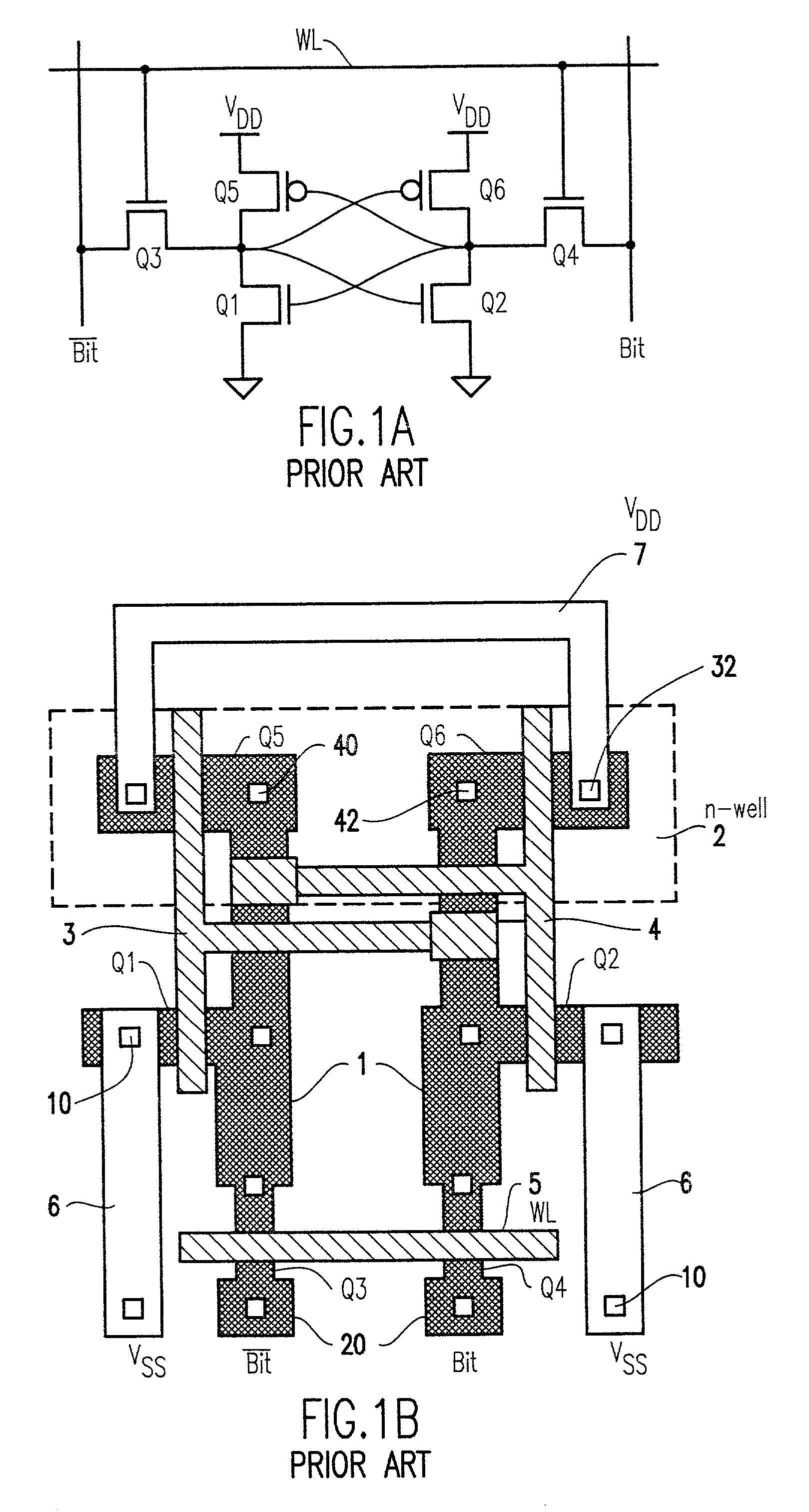
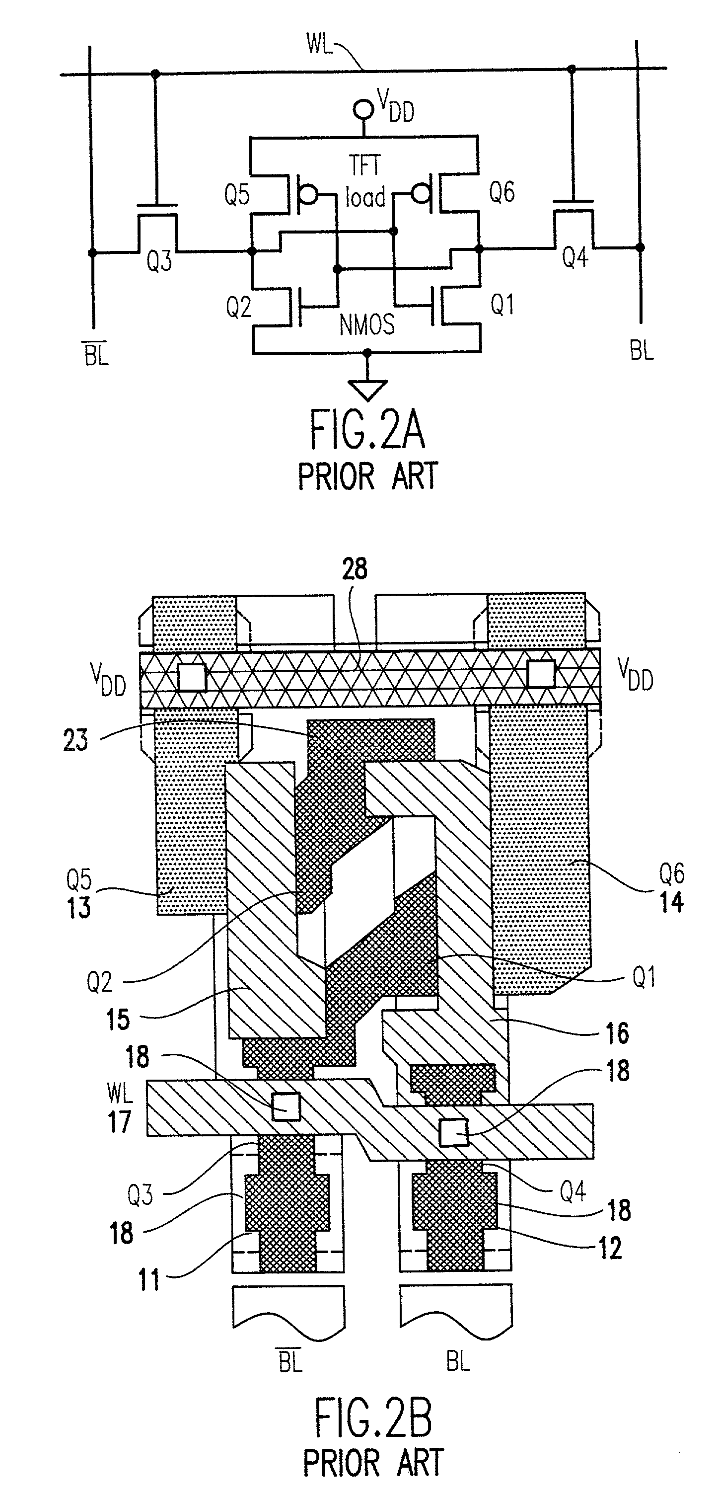
[0023] Referring now to the drawings, and more particularly to FIGS. 1A and 1B, there is shown an example of the prior art of a planar static random access memory (SRAM) arrays. FIG. 1A is a schematic circuit diagram illustrating a standard six transistor CMOS SRAM cell. The NMOS transistors Q1 and Q2 are the "access" devices, the NMOS transistors Q3 and Q4 are "driver" transistors, and the two PMOS transistors Q5 and Q6 are "load" transistors.

[0024] The layout plan view of a standard SRAM cell is shown in FIG. 1B. Q1 and Q2 NMOS transistors are formed by the overlap of the active n-silicon 1 and polysilicon layers 3 and 4. The source contacts 10 of Q1 and Q2 are contacted by metal layer 6 to V.sub.SS or ground. Similarly, Q3 and Q4 are formed by overlap of the active silicon 31 and polysilicon layer 5 which forms the word line (WL). The drain contacts of Q3 and Q4 are connected to bitlines {overscore (Bit)} and Bit, respectively. The PMOS Q5 and Q6 transistors are connected to meta...


PUM


Abstract

The present invention describes the use of two semiconductor layers, a thin film (TF) layer and a bulk Si wafer layer, to make high density and high speed merged logic and memory IC chips. The memory cells use three-dimensional (3D) SRAM structures. Two kinds of 3D logic cells are disclosed. 3D form of the differential cascode voltage switch (DCVS) architecture, and a 3D form of the DCVS with pass gate (DCVSPG) logic architecture. A high density "system on chip" architecture is described. The high density is achieved by locating large PMOS transistors in the TF Si layer, and the fast NMOS transistors in a bulk Si wafer layer. A single process sequence to simultaneously make the logic and memory circuits on the IC chip is also described.

Description

[0001] 1. Field of the Invention[0002] The present invention generally relates to design and fabrication of merged logic circuits and memory arrays on a single semiconductor integrated circuit (IC) chip and, more particularly, to "system on chip" circuits and fabrication methods thereof in which logic circuits use two semi-conductor levels, a thin film level and a bulk silicon (Si) level, and the memory array consists of static random access memory (SRAM).[0003] 2. Background Description[0004] Increasing the density of logic circuits and memory arrays leads to faster circuit performance, smaller integrated circuits (ICs), and hence lower cost per IC. Presently, logic and memory functions are made on separate ICs and overall system speed is limited by communication bandwidth between logic and memory. The performance limit of about 500 MHz is due to communication bandwidth, and is a direct result of logic and memory functions communicating over relatively long distances (millimeters)....

Claims


Application Information

Patent Timeline
Patent Type & Authority Applications(United States)
IPC IPC(8): H01L27/11
CPCH01L27/1108H01L27/0688Y10S257/903H10B10/125
Inventor EMMA, PHILIP GEORGEHWANG, WEIGATES, STEPHEN MCCONNELL
Owner GLOBALFOUNDRIES INC
Learn More