Light-emitting semiconductor device using group III nitride compound

a technology of nitride compound and light-emitting semiconductor, which is applied in the direction of semiconductor devices, electrical equipment, and nanotechnology, etc., can solve the problems of not meeting the required 500 nm wavelength for traffic signals, unable to provide the required wavelength, and unable to obtain the required wavelength peak of 500 nm

Inactive Publication Date: 2001-11-29
TOYODA GOSEI CO LTD
View PDF0 Cites 20 Cited by
  • Summary
  • Abstract
  • Description
  • Claims
  • Application Information

AI Technical Summary

Problems solved by technology

While light, having a peak wavelength of about 500 nm, resulting in a green blue or dark green color, is required for traffic signal lights, the conventional LED 10 is unable to provide that required wavelength.
As a result, the peak wavelength is shifted toward a shorter wavelength in the luminous spectrum and the required wavelength peak of 500 nm cannot be obtained.
Such a peak wavelength does not meet the required 500 nm wavelength for a traffic signal.
Although the peak wavelength of such devices utilizing InGaN or AlGaN is satisfactory, the luminous efficiency of the same is still poor for several reasons.
The emission layer made of InGaN has a poor luminous...

Method used


Image

  • Light-emitting semiconductor device using group III nitride compound
  • Light-emitting semiconductor device using group III nitride compound
  • Light-emitting semiconductor device using group III nitride compound

Examples


example 1

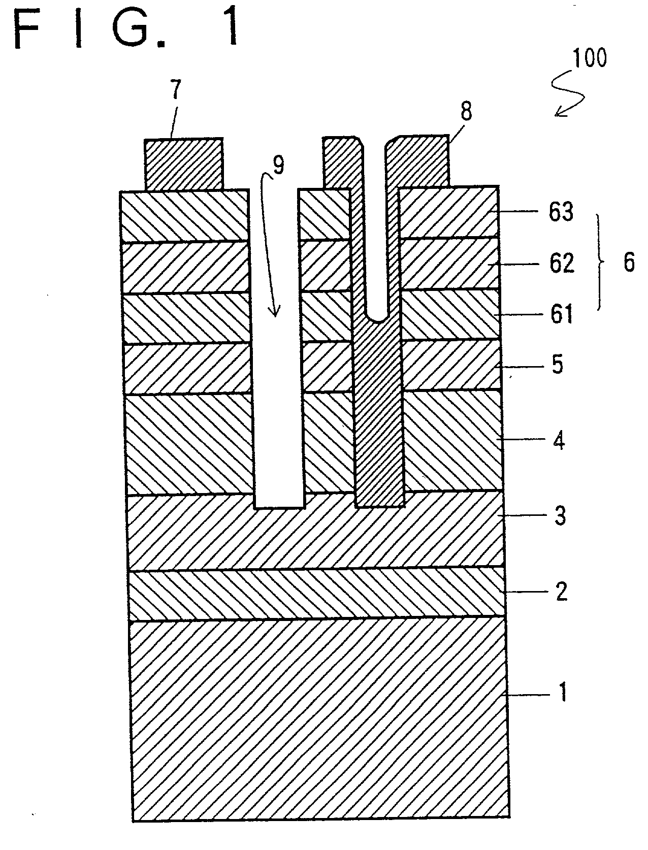
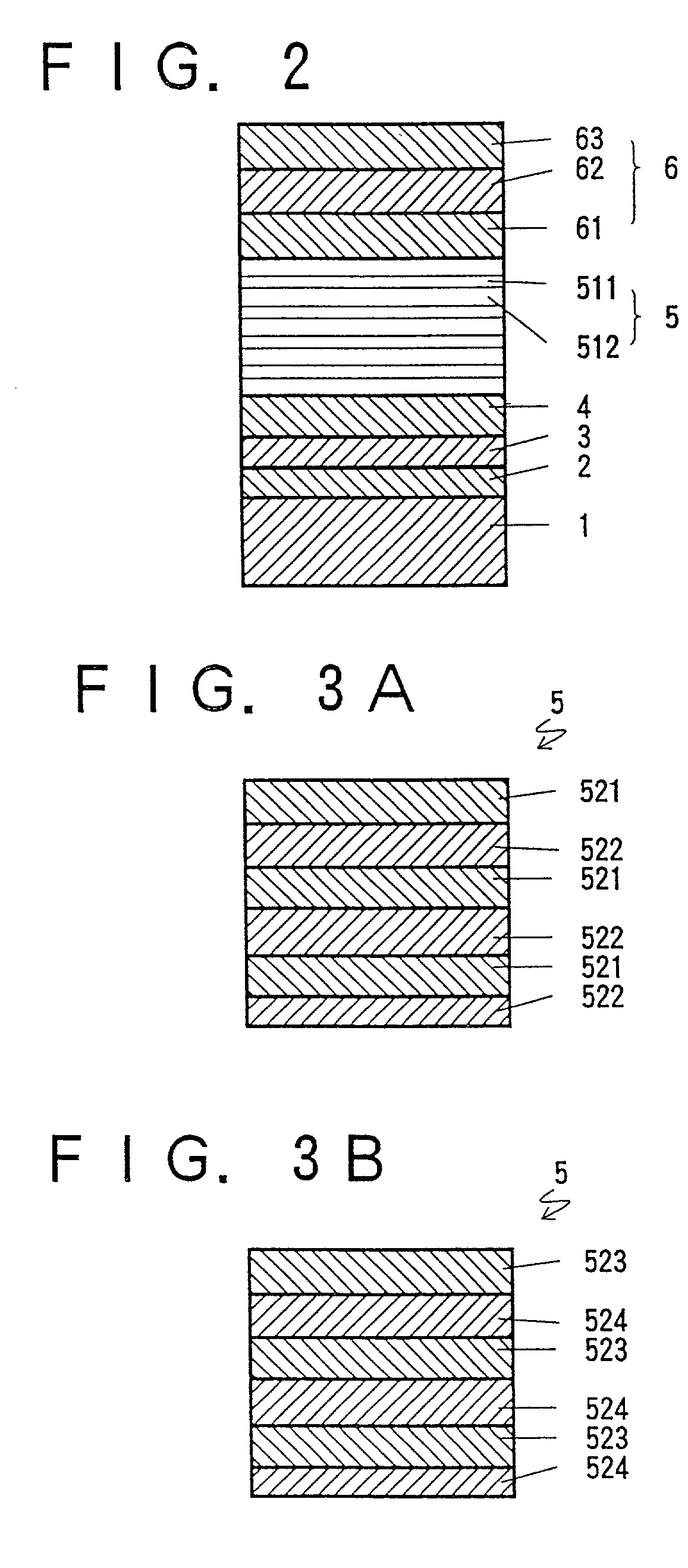
[0049] FIG. 1 shows an LED 100 embodied in Example 1, and FIG. 2 shows a layered structure corresponding to the LED 100 shown in FIG. 1, depicting a multi-layered emission layer 5 in more detail. It has a sapphire (Al.sub.2O.sub.3) substrate 1 upon which a 500 .ANG. in thickness of aluminum nitride (AIN) buffer layer 2 is formed. Consecutively, two n-type layers are formed on the AIN buffer layer 2: about 2.0 .mu.m in thickness of silicon (Si) doped GaN forms an n+-layer 3 of high carrier concentration having an electron concentration of 2.times.10.sup.18 / cm.su-p.3; and about 2.0 .mu.m in thickness of Si-doped Al.sub.x2Ga.sub.1-x2N forms an n-type clad layer 4 having an electron concentration of 8.times.10.sup.17 / cm.sup.3.

[0050] On the n-type clad layer 4, an emission layer 5 about 0.52 .mu.m in thickness and having a multi-layer structure, is formed as shown in FIG. 2. The emission layer 5 includes 13 A-layers 511 and 13 D-layers 512 which are made of magnesium (Mg) and zinc (Zn) d...

example 2

[0064] FIGS. 3A and 3B each show the structure of an emission layer 5 having a multi-layer structure in accordance with Example 2. The emission layer 5 of FIG. 3A has 25 A-layers 521 of Mg- and Zn-doped InGaN and 25 D-layers 522 of Mg- and Si-doped GaN, and that of FIG. 3B has 34 A-layers 523 of Mg- and Zn-doped InGaN and 34 D-layers 524 of Mg- and Si-doped GaN. The differences between the emission layers 5 of Example 2 and Example 1 reside in the thickness of its composite layers and the materials used to form those layers.

[0065] The layers ranging from the sapphire substrate 1 to the n-type clad layer 4 were prepared by above-described processes. As shown in FIG. 3A, about 100 .ANG. in thickness of Mg- and Si-doped GaN, layer 522 (D-layer), was formed as the lowermost layer of the multiple emission layer 5 on the n-type clad layer 4 under conditions controlled by keeping the temperature of the sapphire substrate 1 at 850.degree. C. and concurrently supplying for 2 min. N.sub.2 at ...

example 3

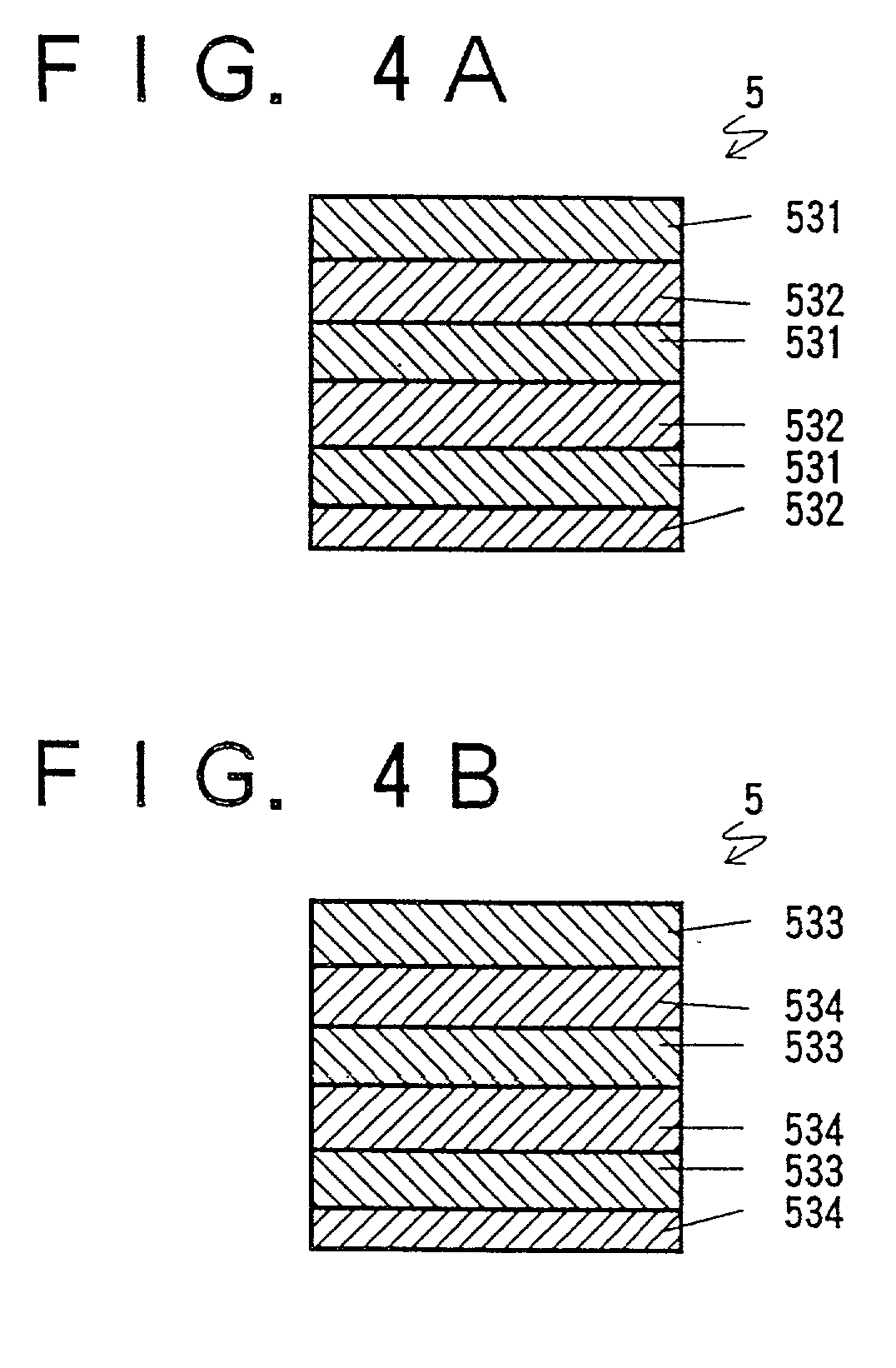
[0069] FIGS. 4A and 4B each show the structure of an multiple emission layer 5 in accordance with Example 3. The emission layer 5 of FIG. 4A has 25 A-layers of Zn-doped In.sub.0.08Ga.sub.0.92N layers 531 having a Zn concentration of 5.times.10.sup.18 / cm.sup.3 and 25 D-layers 532 of Si-doped Al.sub.0.1Ga.sub.0.9N having an Si concentration of 5.times.10.sup.18 / cm.sup.3, and that of FIG. 4B has 25 D-layers 533 of Si-doped In.sub.0.08Ga.sub.0.92N having an Si concentration of 2.times.10.sup.18 / cm.sup.3 and 25 A-layers 534 of Zn-doped Al.sub.0.1Ga.sub.0.9N having a Zn concentration of 1.times.10.sup.18 / cm.sup.3. The A-layers and D-layers were laminated alternately and repeatedly, each having a 100 .ANG. thickness. The D-layer 532 and the A-layer 534 are the lowermost layers. The entire emission layer 5 is about 0.5 .mu.m in thickness and the total number of its composite layers is 50. The other parts of the device were manufactured as described in Example 1.

[0070] The obtained LEDs with...


PUM


Abstract

An emission layer (5) for a light source device is formed to have a multi-layer structure, doped with an acceptor and a donor impurity. The multi-layer structure may include a quantum well (QW) structure or a multi quantum well (MQW) structure (50). With such a structure, a peak wavelength of the light source can be controlled, because the distances between atoms of the acceptor and the donor impurities are widened. Several arrangements can be made by, e.g., altering the thickness of each composite layer of the multi-layer structure, altering their composition ratio, forming undoped layer 5 between the impurity doped layers, and so forth. Further, luminous intensity of ultra violet color can be improved, because doping the donor impurity and the acceptor impurity realizes a donor-acceptor emission mechanism and abundant carriers. Several arrangements can be made by, e.g., optimizing the materials of the composite layers, optimizing their composition ratios, optimizing their lattice constants, and so forth to further enhance the luminous intensity of the light source.

Description

[0001] 1. Field of the Invention[0002] The present invention relates to a light-emitting semiconductor diode (LED) and a laser diode (LD) that use a Group III nitride compound and that has a multiple emission layer. Especially, the invention relates to an LED and an LD having an improved emission efficiency in the visible short wavelength region from the green blue to blue color and in the ultra violet region.[0003] 2. Description of the Related Art[0004] It has been known that an aluminum gallium indium nitride (AlGaInN) compound semiconductor may be used to obtain a light-emitting diode (LED) or a laser diode (LD) which emits blue and ultra violet color light. This semiconductor device is useful because of its high luminous efficiency resulting from direct electron transition and because of its ability to emit blue light, which is one of the three primary colors.[0005] By irradiating an electron beam and carrying out heat treatment, a magnesium (Mg) doped i-layer is changed into a...

Claims


Application Information

Patent Timeline
IPC IPC(8): H01L33/06H01L33/32
CPCB82Y20/00H01L33/06H01L33/325
Inventor KOIKE, MASAYOSHIASAMI, SHINYA
Owner TOYODA GOSEI CO LTD
Why Eureka
Try Eureka