Chemically synthesized and assembled electronic devices

a technology of electronic devices and components, applied in the direction of superconductor devices, instruments, and semiconductor/solid-state device details, can solve the problem of affecting the rate of charge transport across the wire junction, and achieve the effect of simple and inexpensive implementation

Inactive Publication Date: 2001-12-27
HEWLETT PACKARD CO +1
View PDF13 Cites 95 Cited by
  • Summary
  • Abstract
  • Description
  • Claims
  • Application Information

AI Technical Summary

Benefits of technology

0007] In accordance with the present invention, a route to the fabrication of electronic devices is provided, in which the devices consist of two crossed wires sandwiching an electrically addressable molecular species. The approach is extremely simple and inexpensiv

Problems solved by technology

Oxidation or reduction will affect the tunneling distance or the tunneling barrier height between the two wires, thereby exponentially

Method used


Image

  • Chemically synthesized and assembled electronic devices
  • Chemically synthesized and assembled electronic devices
  • Chemically synthesized and assembled electronic devices

Examples


examples

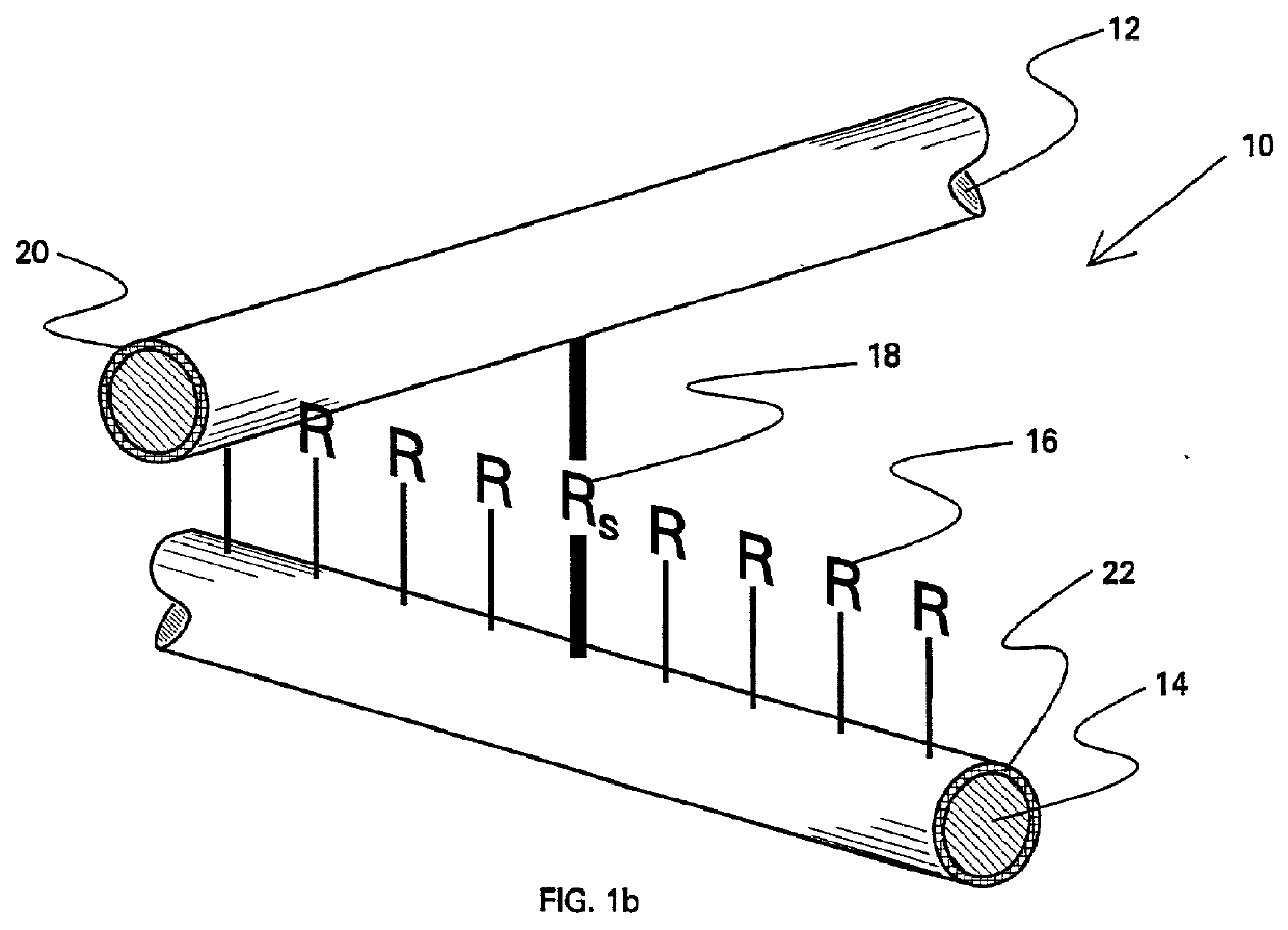
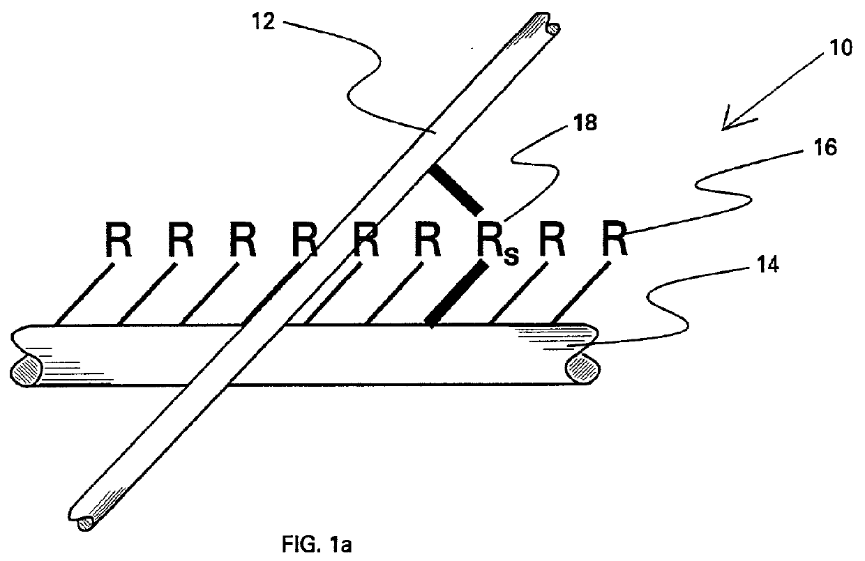
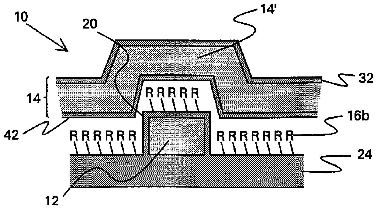
[0069] The present invention was reduced to practice to make a molecular switch-based based device that could be configured as an electrically configurable read-only-memory, nonlinear logic gates that operated as diode-based logic, or a signal routing device. The device was made according to the method described in FIGS. 2A-2D, with the following modifications: A 5 micrometer wide aluminum wire 12 was deposited on a silica substrate 24 using conventional lithographic procedures. The wire 12 was provided with an oxide coating 14 of Al.sub.2O.sub.3, which naturally formed to a thickness of about 1.0 to 1.5 nm when the aluminum wire was exposed to air. One of the molecular species shown in FIGS. 4A-4C was dissolved in tetrahydrofuran solvent, prepared as a Langmuir monolayer, and transferred as a Langmuir-Blodgett single molecular monolayer film 16 that covered the Al wire 12 and the silica substrate 24. The molecular compounds shown in FIGS. 4A-4C are from a class of molecular compoun...


PUM

PropertyMeasurementUnit
Angleaaaaaaaaaa
Thicknessaaaaaaaaaa
Diameteraaaaaaaaaa

Abstract

A route to the fabrication of electronic devices is provided, in which the devices consist of two crossed wires sandwiching an electrically addressable molecular species. The approach is extremely simple and inexpensive to implement, and scales from wire dimensions of several micrometers down to nanometer-scale dimensions. The device of the present invention can be used to produce crossbar switch arrays, logic devices, memory devices, and communication and signal routing devices. The present invention enables construction of molecular electronic devices on a length scale than can range from micrometers to nanometers via a straightforward and inexpensive chemical assembly procedure. The device is either partially or completely chemically assembled, and the key to the scaling is that the location of the devices on the substrate are defined once the devices have been assembled, not prior to assembly.

Description

[0001] The present application is related to the following applications: Ser. Nos. ______ ("Molecular Wire Crossbar Interconnects for Signal Routing and Communications") [PD-10981966-1]; ______ ("Molecular Wire Crossbar Memory") [PD-10981968-1]; ______ ("Molecular Wire Crossbar Logic") [PD-10981969-1]; ______ ("Demultiplexer for a Molecular Wire Crossbar Network") [PD-10981970-1]; and ______ ("Molecular Wire Transistors") [PD-10981967-1], all filed on even date herewith. The present application is the foundational application, upon which the related applications depend for construction of the various devices and apparati disclosed and claimed therein.[0003] The present invention relates generally to electronic devices whose functional length scales are measured in nanometers, and, more particularly, to simple devices used as building blocks to form more complicated structures, and to the methods for forming such devices. Devices both of micrometer and nanometer scale may be construc...

Claims


Application Information

Patent Timeline
IPC IPC(8): B81B7/04B82B1/00G01R31/28G11C13/02H01L21/00H01L23/532H01L27/10H01L29/861H01L51/00H01L51/05H01L51/30H01L51/40
CPCB82B1/00B82Y10/00B82Y30/00G11C13/0009G11C13/0014G11C13/02G11C2213/72G11C2213/77G11C2213/81H01L27/10H01L51/0595Y10S977/936Y10S977/704Y10S977/705H10K10/701
Inventor HEATH, JAMES R.WILLIAMS, R. STANLEYKUEKES, PHILIP J.
Owner HEWLETT PACKARD CO
Why Eureka
Try Eureka