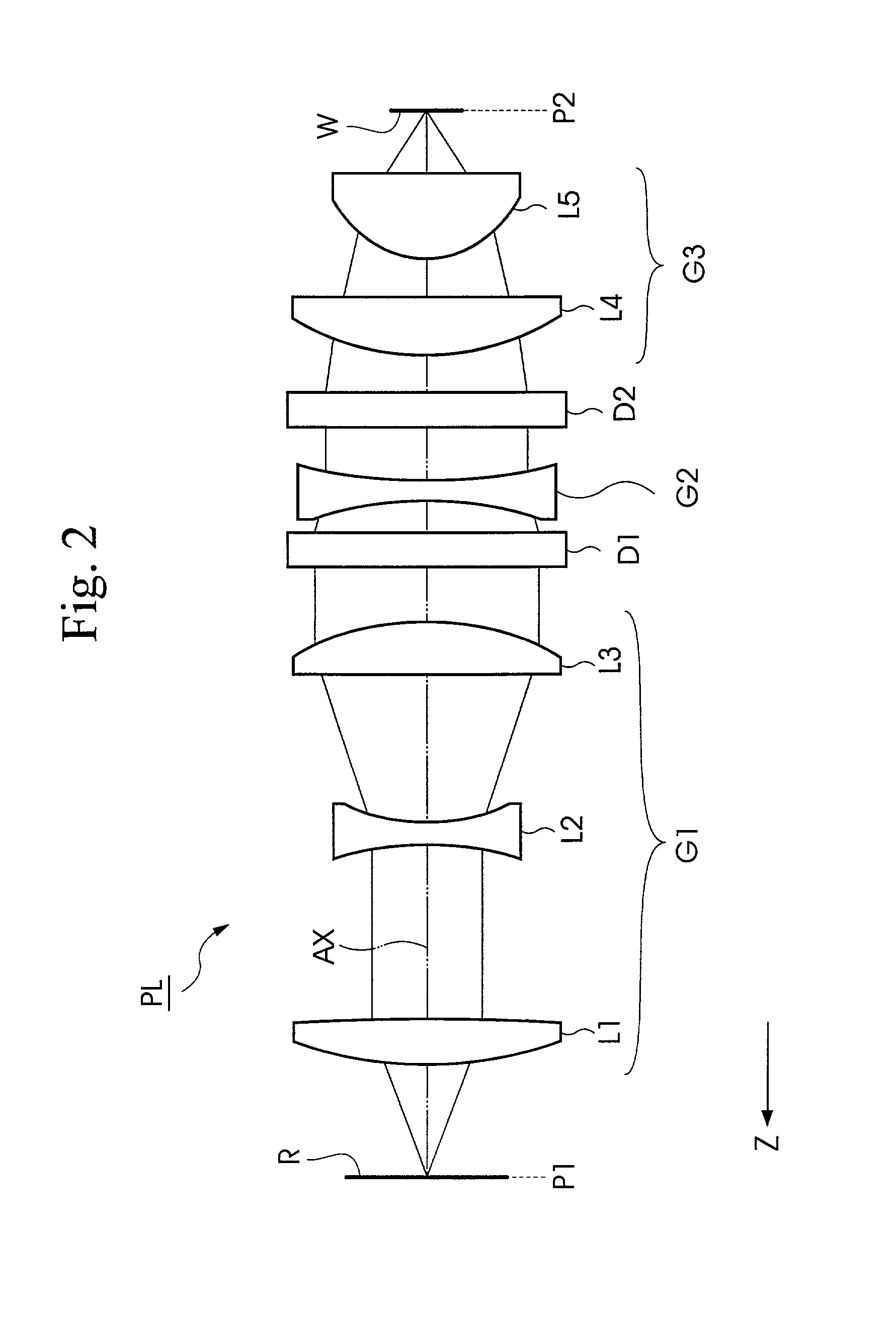
[0015] According to this projection optical system, an optical system having a
negative power is arranged in the optical path between the first diffractive optical element and the second diffractive optical element, so as to adjust the
angle of incidence of the
luminous flux which is incident to the second diffractive optical element. Therefore, the
luminous flux can be diffracted according to the
diffraction characteristic of the second diffractive optical element, and as a result, the image on the first plane can be formed on the second plane with high precision. Hence, the system is especially suitable for forming an image of a minute pattern, in particular, a pattern of 0.1 .mu.m or less on the second plane.
[0017] According to this projection optical system, the axial
luminous flux on the first plane is converted to a substantially parallel luminous flux, and shone onto the first diffractive optical element, and the axial luminous flux on the first plane via the first diffractive optical element is again converted to a substantially parallel luminous flux and guided to the second diffractive optical element. As a result, the image on the first plane can be formed on the second plane with high precision. Moreover, the first diffractive optical element and the second diffractive optical element have a
chromatic aberration characteristic opposite to that of a
chromatic aberration caused by the front optical system, the rear optical system and the optical system having a
negative power, and do not affect the Petzval's condition. Hence the chromatic aberration can be corrected favorably. As a result, the system is especially suitable for forming an image on the first plane on the second plane with high precision. Furthermore, since correction of chromatic aberration is performed only by the diffractive optical element, several lenses arranged in the optical path for correcting the chromatic aberration are not required, thereby keeping down cost increase. Also, even if chromatic aberration cannot be corrected by lenses, due to a restriction on the
glass material of the lenses, chromatic aberration can be corrected by using a diffractive optical element having an aberration characteristic opposite to that of lenses. Furthermore, since two diffractive optical elements, namely the first diffractive optical element and the second diffractive optical element, are used to obtain a power required for correction of chromatic aberration by each diffractive optical element, even if values of chromatic aberration in the front optical system, the rear optical system and the optical system having a negative power are varied, chromatic aberration can be properly corrected.
[0019] According to this projection optical system, by satisfying the above described conditions, a projection optical system having a large numerical aperture, but having no imaging performance degradation due to the angular characteristic can be realized. Hence sufficient correction of chromatic aberration can be realized. Moreover, by satisfying the above described conditions, the
pitch of the diffractive optical elements is not refined so much, and diffractive optical elements having a relatively wide
pitch and which are easy to manufacture can be used.
[0020] Furthermore, a third aspect of the present invention is a projection optical system (PL) having a plurality of optical elements arranged along an optical path between a first plane (P1) and a second plane (P2) for forming an image on the first plane (P1) on the second plane (P2), wherein at least one diffractive optical element (D1, D2) having a
diffraction pattern surface (PL1, PL11) formed on one surface and a correction surface (PL2, PL22) formed on an other surface is arranged along the optical path, and the correction surface (PL2, PL12) corrects a manufacturing error on the
diffraction pattern surface (PL1, PL11).
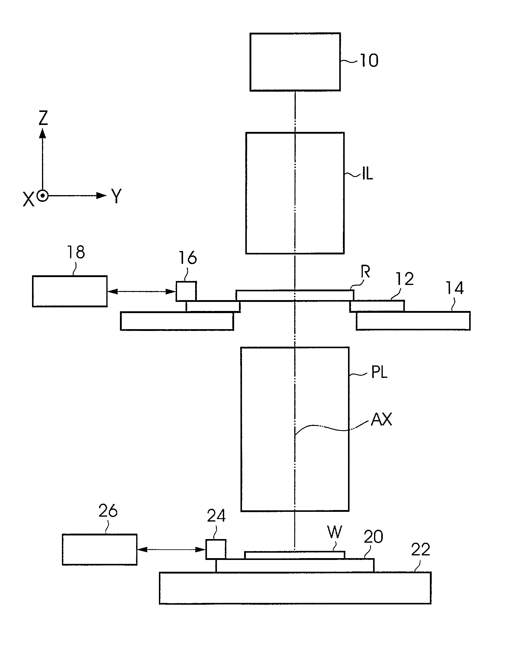
[0032] According to this exposure apparatus, the pattern image formed on the
mask arranged on the first plane can be formed with high precision on the photosensitive substrate arranged on the second plane. As a result, the apparatus is extremely suitable for forming a minute pattern, especially, a minute pattern of 0.1 .mu.m or less on the
wafer.
[0034] According to this manufacturing method for micro devices, as in the above described exposure apparatus, the pattern image formed on the mask arranged on the first plane can be formed with high precision on the photosensitive substrate arranged on the second plane. As a result, the method is extremely suitable for manufacturing micro devices where it is necessary to form a minute pattern, especially, a minute pattern of 0.1 .mu.m or less on the
wafer.

