Supercharge Your Innovation With Domain-Expert AI Agents!

Liquid crystal display device and method of manufacturing the same

a liquid crystal display device and active matrix technology, applied in the direction of identification means, instruments, optics, etc., can solve the problems of small visibility angle, adversely affecting the color filter layer, and small visibility angle of tn type liquid crystal display devi

Inactive Publication Date: 2002-02-28
NEC CORP
View PDF0 Cites 27 Cited by
  • Summary
  • Abstract
  • Description
  • Claims
  • Application Information

AI Technical Summary

Benefits of technology

This configuration prevents charge-up in the color filter layer, suppressing color shades and enhancing the visibility angle by maintaining the electric field's effect solely on the liquid crystal layer, thereby improving display characteristics without affecting the color filter.

Problems solved by technology

However, the inherent behavior of the liquid crystal voltages under voltage-applied state causes a problem that the angle of visibility of the TN type liquid crystal display device is small.
The problem that the angle of visibility is small is particularly remarkable in the rise-up direction of the liquid crystal molecules under a half tone display state.
However, in the IPS system, the color filter layer is disposed between the liquid crystal layer and the counter substrate, and thus the electric field which will be formed when potential is applied between the source electrode and the drawn-out common electrode adversely affects the color filter layer and degrades the display characteristic of the active matrix type liquid crystal display device.
When the color filter layer charges up, undesired electric field is applied to the liquid crystal molecules below the charge-up area of the color filter layer at all times, so that the display characteristic is adversely effected.

Method used


Image

  • Liquid crystal display device and method of manufacturing the same
  • Liquid crystal display device and method of manufacturing the same
  • Liquid crystal display device and method of manufacturing the same

Examples


first embodiment

[0151] [First Embodiment]

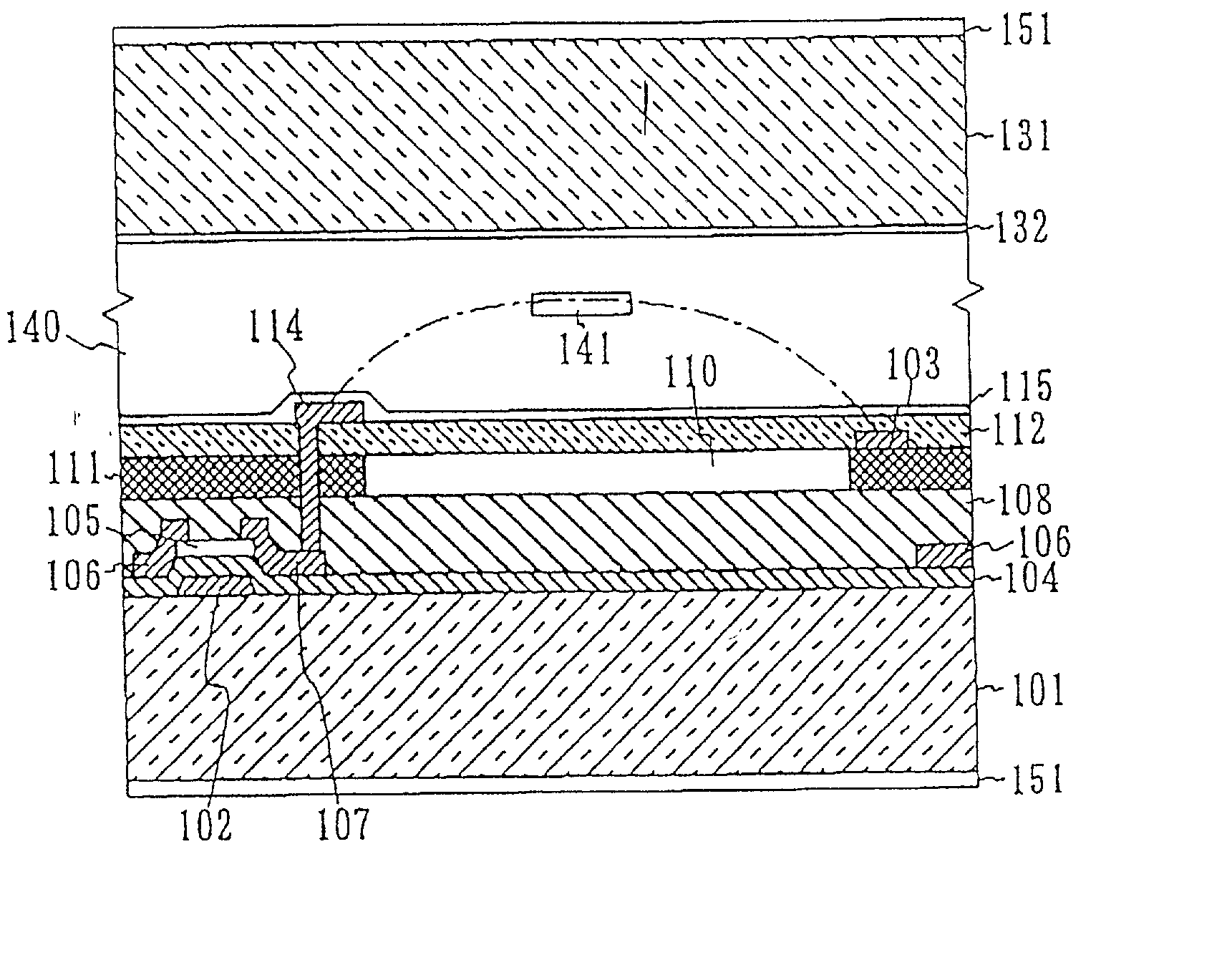
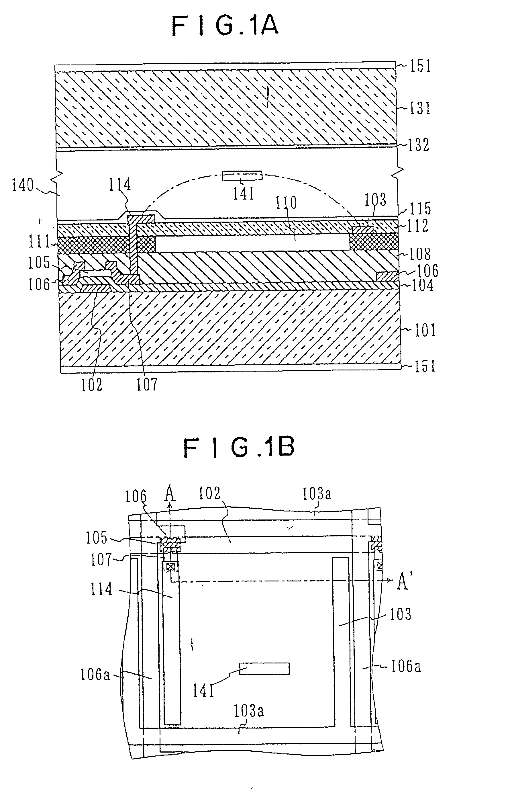
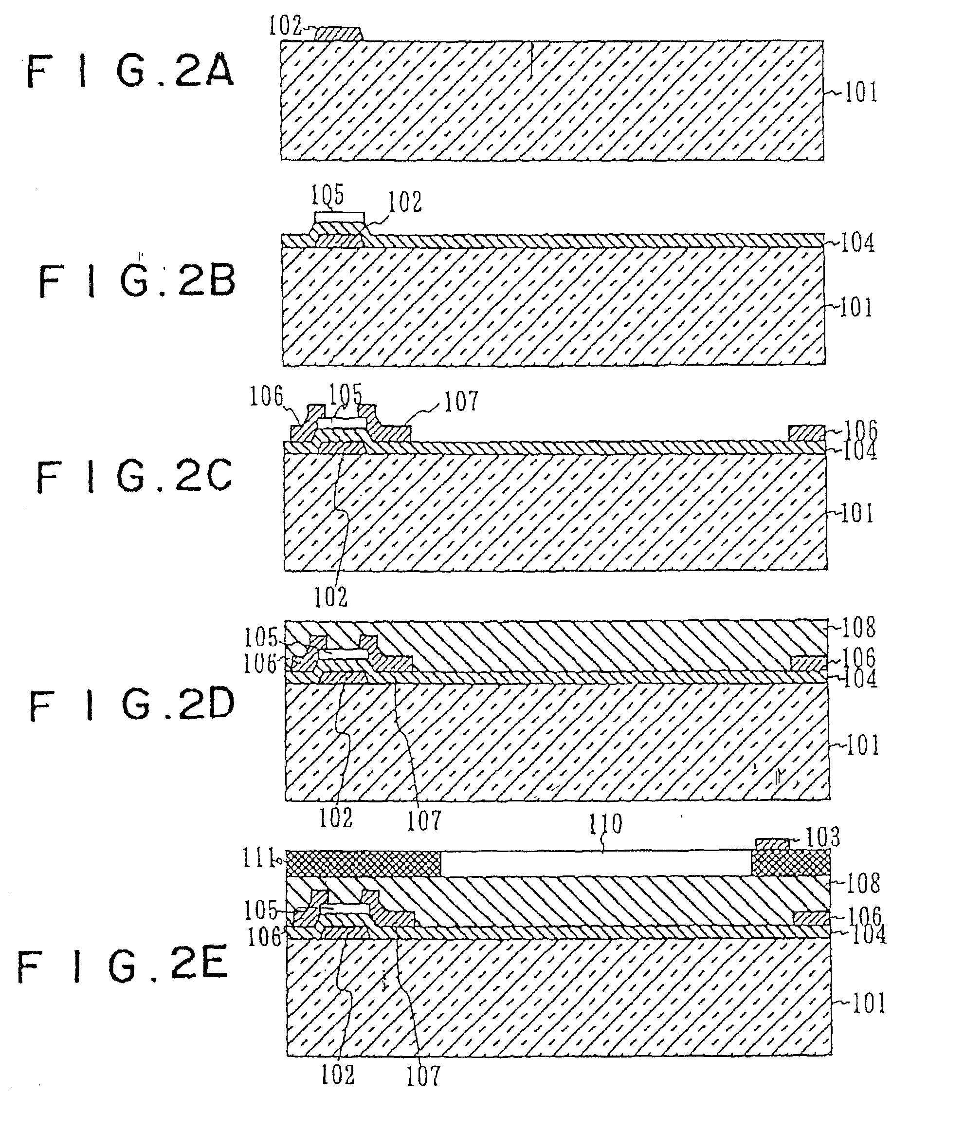
[0152] A substrate having an array of amorphous silicon thin film transistors (TFT) was formed on a glass substrate by repeating both of a film forming process and a lithography process. The TFT array comprises a gate--chrome layer, a silicon nitride--gate insulating layer, an amorphous silicon-semiconductor layer, a drain / source--molybdenum layer which were arranged from the substrate side in this order (see FIG. 2C). Thereafter, a protection film was formed of silicon nitride so as to cover the above layers.

[0153] Subsequently, for example a color filter layer of green was coated on the protection layer, heated and dried and formed by photolithography. The same process was repeated to form red, blue color filter layers, thereby forming a color filter layer. A light shielding portion was formed by using resin containing black pigment in the same manner. Thereafter, a common electrode was formed of chrome, and then an overcoat layer of acrylic resin was coat...

second embodiment

[0159] (Second Embodiment)

[0160] As in the case of the first embodiment, an array of amorphous silicon thin film transistors (TFT) was formed by repeating both the film forming process and the lithography process. TFT comprised a gate--chrome layer, a silicon nitride--gate insulating layer, a amorphous silicon--semiconductor layer and a drain / source--molybdenum layer which were arranged from the substrate side in this order as in the case of the first embodiment.

[0161] A protection film of silicon nitride was formed so as to cover the above layers, and red, blue and green color filter layers were formed in the same manner as the first embodiment. After a common electrode was formed of chrome, an overcoat layer of acrylic resin was coated and heated for one hour at 200.degree. C.

[0162] Subsequently, a through hole was formed so as to extend to the source electrode, and a pixel electrode is formed by using ITO SE1211 produced by Nissan Chemical Company was coated as a vertical orienta...


PUM

PropertyMeasurementUnit
thicknessaaaaaaaaaa
transparentaaaaaaaaaa
areasaaaaaaaaaa

Abstract

In a liquid crystal display device comprising a first substrate 101 having a color filter, a second substrate 131 and a liquid crystal layer disposed therebetween, a color filter layer 110 is disposed on a protection film 108 of a thin film transistor formed on the first substrate 101 so as to be partitioned by a light shielding portion 111, and a common electrode 103 is disposed thereon. A pixel electrode to be connected to a source electrode 107 is disposed through a through hole formed in an overcoat layer (interlayer separation film) 112. On the first substrate below the color filter layer 110 are provided plural scan signal electrodes, plural video signal electrodes crossing the scan signal electrodes in a matrix form, plural thin film transistors formed in association with the crossing points between the electrodes. Each pixel is provided with a common electrode 103 which is connected over plural pixels through a common electrode wire to supply reference potential, and a pixel electrode 114 which is connected to the corresponding thin film transistor and disposed so as to confront the common electrode in the pixel area.

Description

[0001] 1. Field of the Invention[0002] The present invention relates to an active matrix type liquid crystal display device which thin film transistors (TFT) are arranged in a matrix form and these thin film transistors are used as switching elements.[0003] 2. Description of the Related Art[0004] An active matrix type TFT (Thin Film Transistor: hereinafter abbreviated as "TFT") liquid crystal display device in which TFTs are formed in a matrix arrangement on a glass substrate and these TFTs are used as switching elements has been developed as a high-quality flat-face display. In a twisted nematic (hereinafter abbreviated as "TN") type active matrix crystal display device which has been hitherto widely used, transparent electrodes which are formed on two glass substrates so as to confront each other are used as electrodes for driving a liquid crystal layer. By applying a voltage to liquid crystal molecules which are arranged in parallel to the substrate surface under non-voltage appl...

Claims


Application Information

Patent Timeline
Patent Type & Authority Applications(United States)
IPC IPC(8): G09F9/30G02F1/133G02F1/1337G02F1/1343G02F1/136G02F1/1365G02F1/1368H01L21/336H01L29/786
CPCG02F1/134363G02F1/1337
Inventor SAKAMOTO, MICHIAKIWATANABE, TAKAHIKOIHARA, HIROFUMIKIKKAWA, HIRONORIOKAMOTO, MAMORUNAKATA, SHINICHIYAMAMOTO, YUJISUZUKI, MASAYOSHISUZUKI, TERUAKIISHII, TOSHIYAKANOH, HIROSHI
Owner NEC CORP
Features
  • R&D
  • Intellectual Property
  • Life Sciences
  • Materials
  • Tech Scout
  • Unparalleled Data Quality
  • Higher Quality Content
  • 60% Fewer Hallucinations
Learn More