Metallic undercoating for solder materials

a technology of solder materials and undercoating, which is applied in the direction of welding/cutting media/materials, soldering media, electrical equipment, etc., can solve the problems of brittle intermetallics forming with solder materials, and achieve the effect of easy production and easy wetting

Inactive Publication Date: 2002-04-25
FRAUNHOFER GESELLSCHAFT ZUR FOERDERUNG DER ANGEWANDTEN FORSCHUNG EV
View PDF0 Cites 13 Cited by
  • Summary
  • Abstract
  • Description
  • Claims
  • Application Information

AI Technical Summary

Benefits of technology

[0014] It is the object of the present invention to provide a semiconductor substrate with an underbump metallization in the case of which the underbump metallization is easy to produce and can easily be wetted with the solder material to be applied.
[0015] It is also an object of this invention to provide a method of forming a semiconductor substrate with an underbump metallization in the case of which the underbump metallization is easy to produce and can easily be wetted with solder material to be applied.
[0017] In comparison with the prior art described hereinbefore, the present invention offers the advantage that no second metallic layer is required for obtaining a good wettability with a solder material, whereby the production method for such metallic undercoatings is substantially simplified.
[0018] Another advantage is to be seen in the fact that by avoiding the second metallic layer the formation of brittle intermetallics is prevented.

Problems solved by technology

A disadvantage entailed by the use of such metallizations is that a further metallic layer consisting of copper, nickel, etc. has to be applied to the titanium-tungsten layer so as to provide a wettable base for the solder bumps or for die bonding.
Another disadvantage is that the application of the second metallic layer results in the formation of brittle intermetallics with the solder material.

Method used


Image

  • Metallic undercoating for solder materials
  • Metallic undercoating for solder materials

Examples


first embodiment

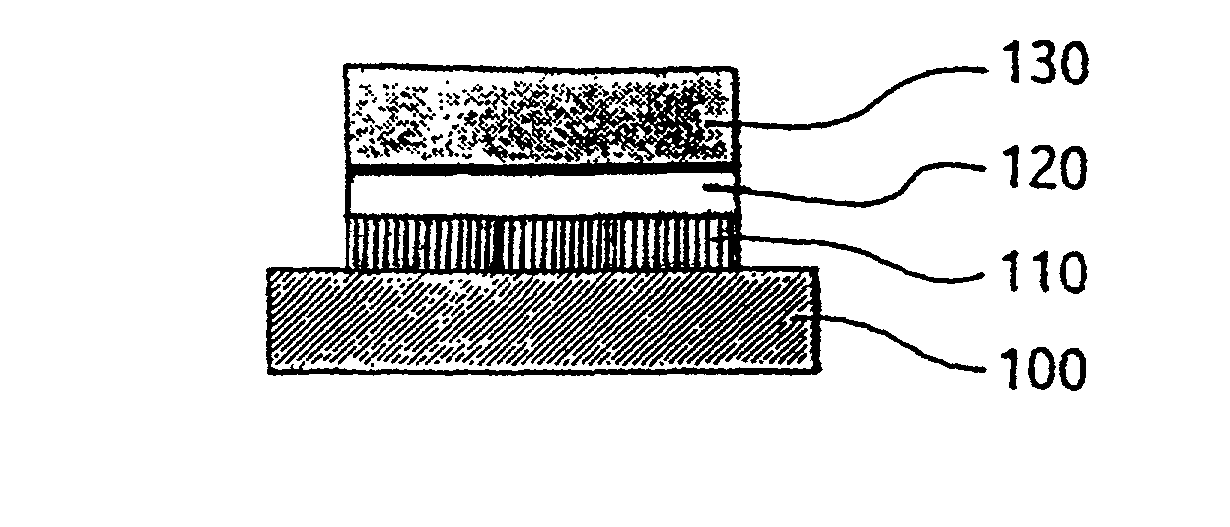
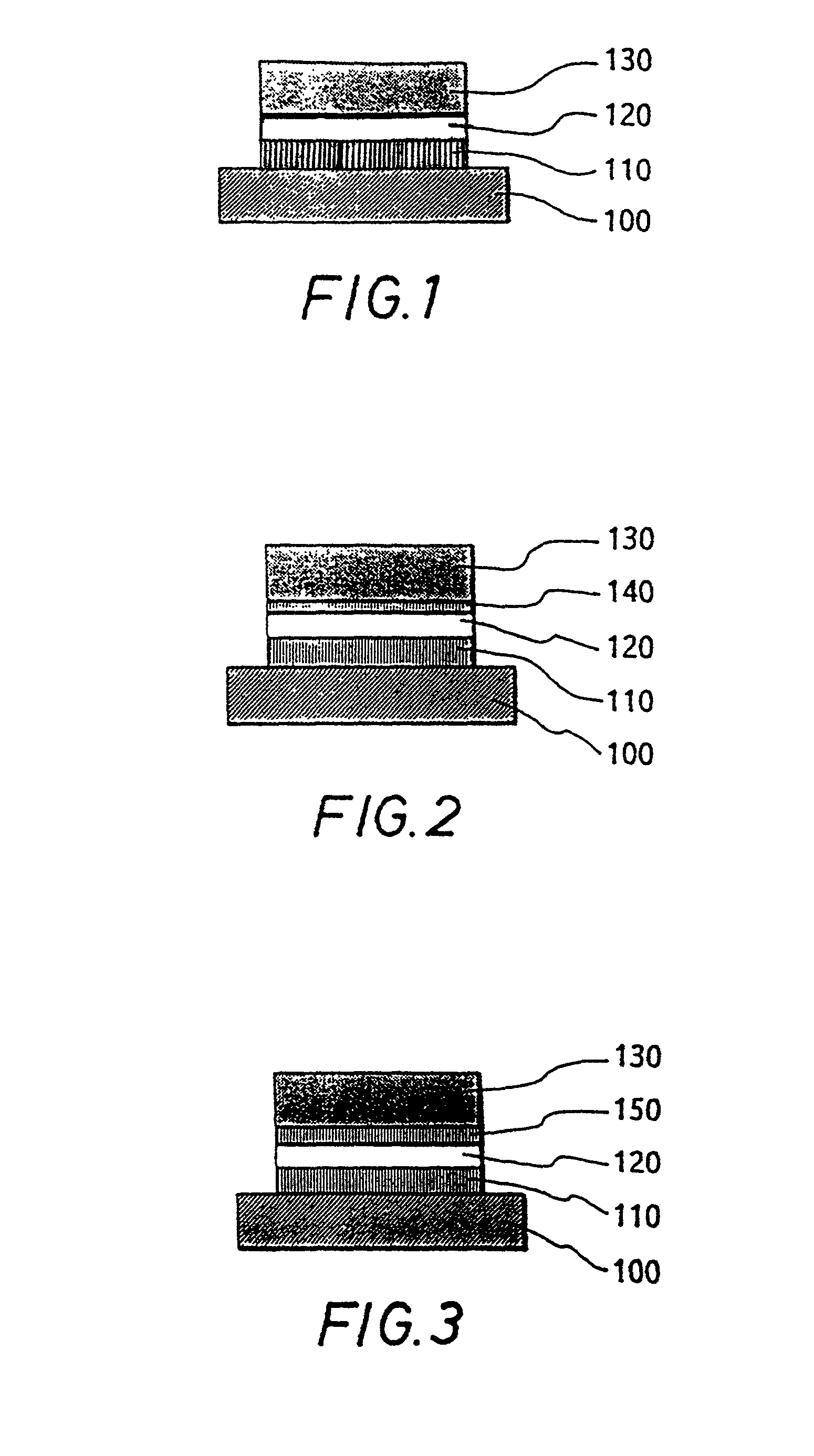
[0024] FIG. 1 shows the present invention. A substrate base 100 has arranged thereon a connection layer 110 on which a titanium diffusion barrier 120 is arranged. This titanium diffusion barrier 120 forms a metallic undercoating for a solder 130 to be applied to this titanium diffusion barrier 120.

[0025] The titanium diffusion barrier 120 offers a wettable basis for various solder materials 130. Possible solder materials include: lead alloys, silver alloys, tin alloys, gold alloys, bismuth alloys, antimony alloys, indium, and indium alloys. More specific examples include: Pb / Sn, Au / Sn, In solders, Sn / Ag, and Sn / Bi.

[0026] Possible solder application methods are mechanical and galvanic bumping, dip soldering and vapor deposition.

[0027] The metallic undercoating according to the present invention is, however, not limited to solder application methods of this type, but it is also adapted to be used for what is termed die bonding.

[0028] In the embodiment shown in FIG. 1, only one step is...

second embodiment

[0032] The second embodiment shown in FIG. 2 corresponds essentially to the embodiment according to FIG. 1. It includes, however, a metal layer 140, such as gold, which is arranged between the titanium diffusion barrier 120 and the solder material 130.

[0033] Due to the fact that titanium has a strong affinity for gold, it forms various so-called intermetallics with gold. These intermetallics are easily wettable by various solder materials.

embodiment 1

[0034] Possible solder materials have already been described on the basis of embodiment 1 in FIG. 1.

[0035] Due to the use of the metal layer 140, oxidation of the titanium diffusion barrier 120 is avoided during a production process of the metallic undercoating. The layer 140 is not limited to gold, but any other metal having a sufficient affinity for titanium is just as suitable to be used as said layer 140. These metals include: silver, silver alloys, platinum, palladium, titanium-aluminum alloys, nickel-aluminum alloys, titanium-nickel-aluminum alloys, titanium-nitrogen alloys, and titanium-niobium alloys.

[0036] The embodiment shown in FIG. 3 corresponds essentially to FIG. 2 with the exception that the titanium diffusion barrier 120 and the solder material 130 have arranged between them a metallic layer 150 instead of the metal layer 140.

[0037] Titanium forms various intermetallics with tin so that a good wettability for solder materials exists again.

[0038] During the production...


PUM

PropertyMeasurementUnit
semiconductoraaaaaaaaaa
affinityaaaaaaaaaa
vacuumaaaaaaaaaa

Abstract

A semiconductor substrate has an underbump metallization for solder materials. The semiconductor substrate has applied thereto a titanium layer serving as a diffusion barrier and as a wettable surface for the solder-material bump. The solder-material bump is adapted to be applied directly to said diffusion barrier.

Description

[0001] This application is a Continuation-in-Part of U.S. patent application Ser. No. 08 / 913,387, filed August 27, 1997; which is a nationalization of PCT Application PCT / DE96 / 00084, dated Jan. 16, 1996.[0002] 1. Field of the Invention[0003] The present invention refers to a semiconductor substrate with an underbump metallization for various solder materials.[0004] 2. Background Art[0005] One pre condition for such a metallization is that it is easily wettable for the solder material to be applied and that it acts simultaneously as a diffusion barrier. and as a diffusion barrier. The material used for this purpose is titanium-tungsten which is applied by atomization or sputtering.[0006] A disadvantage entailed by the use of such metallizations is that a further metallic layer consisting of copper, nickel, etc. has to be applied to the titanium-tungsten layer so as to provide a wettable base for the solder bumps or for die bonding. Another disadvantage is that the application of the ...

Claims


Application Information

Patent Timeline
Patent Type & Authority Applications(United States)
IPC IPC(8): B23K35/00
CPCB23K35/001H01L2224/04026H01L2924/09701H01L2924/01327H01L2924/10253H01L2924/00
Inventor ZAKEL, ELKEKALLMAYER, CHRISTINENAVE, JENS
Owner FRAUNHOFER GESELLSCHAFT ZUR FOERDERUNG DER ANGEWANDTEN FORSCHUNG EV
Why Eureka
Try Eureka