Trench isolation structure having a curvilinear interface at upper corners of the trench isolation region, and method of manufacturing the same
a technology of trench isolation and curvilinear interface, which is applied in the direction of semiconductor devices, electrical equipment, basic electric elements, etc., can solve the problems of silicon dislocation in the semiconductor substrate, the oxide layer buried in the trench expands, etc., and achieves the effect of suppressing leakage curren
- Summary
- Abstract
- Description
- Claims
- Application Information
AI Technical Summary
Benefits of technology
Problems solved by technology
Method used
Image

Examples
first embodiment
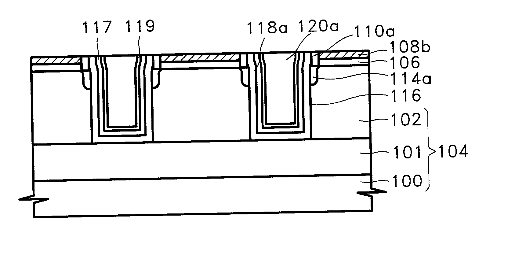
[0025] FIG. 6 shows trench isolation structure in which a trench 116 extends into a semiconductor substrate 104 from an upper surface of the substrate, and a trench isolation layer occupies the trench to electrically isolate active regions. In this embodiment, the trench isolation layer comprises a first oxide layer 120b, a buffer layer 118a, and a thermal oxide layer 114a. The first oxide layer is buried in the trench 116 of the semiconductor substrate 104 as surrounded by the buffer layer 118a. The thermal oxide layer 114a contacts the buffer layer 118a at the upper corners of the substrate 104 where the upper surface of the substrate 104 and inner walls of the substrate 104 that define the trench 116 meet. Thus, the trench isolation layer and the semiconductor substrate contact each other at the upper corners of the substrate 104. This interface between the trench isolation layer and the semiconductor substrate has a rounded vertical sectional profile. More specifically, the inte...
embodiment 1
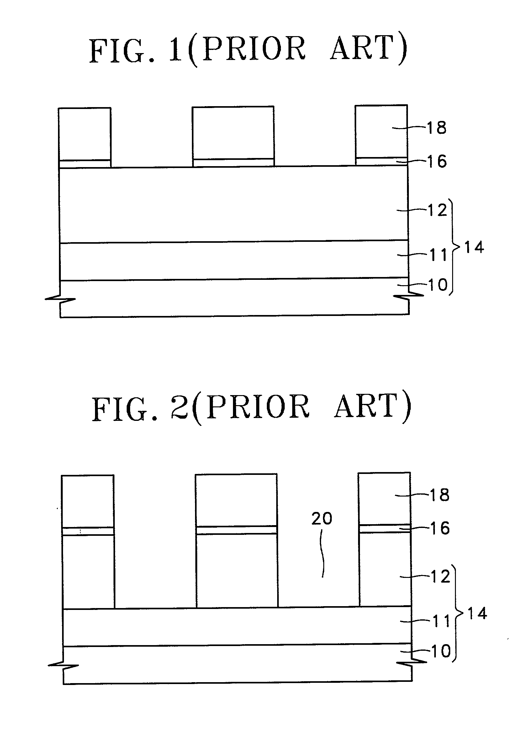
[0032] FIGS. 8-14 show steps in one method of manufacturing a trench isolation layer according to the present invention. Referring to FIG. 8, a pad oxide layer and a hard mask layer are sequentially deposited over a semiconductor substrate 104. The semiconductor substrate 104 has a silicon-on-insulator structure in which a silicon substrate 100, a buried oxide layer 101, and a monocrystalline silicon layer 102 are sequentially disposed one atop the other. The pad oxide layer may be a silicon oxide layer having a thickness of about 50-300 .ANG., and preferably, of about 100 .ANG.. The hard mask layer preferably has a thickness of about 1,000-3,000 .ANG.. The hard mask layer may consist of a silicon nitride layer, a composite layer of silicon nitride and an oxide sequentially disposed one atop the other, or a composite layer in which either an anti-reflective material or an anti-reflective coating is incorporated.
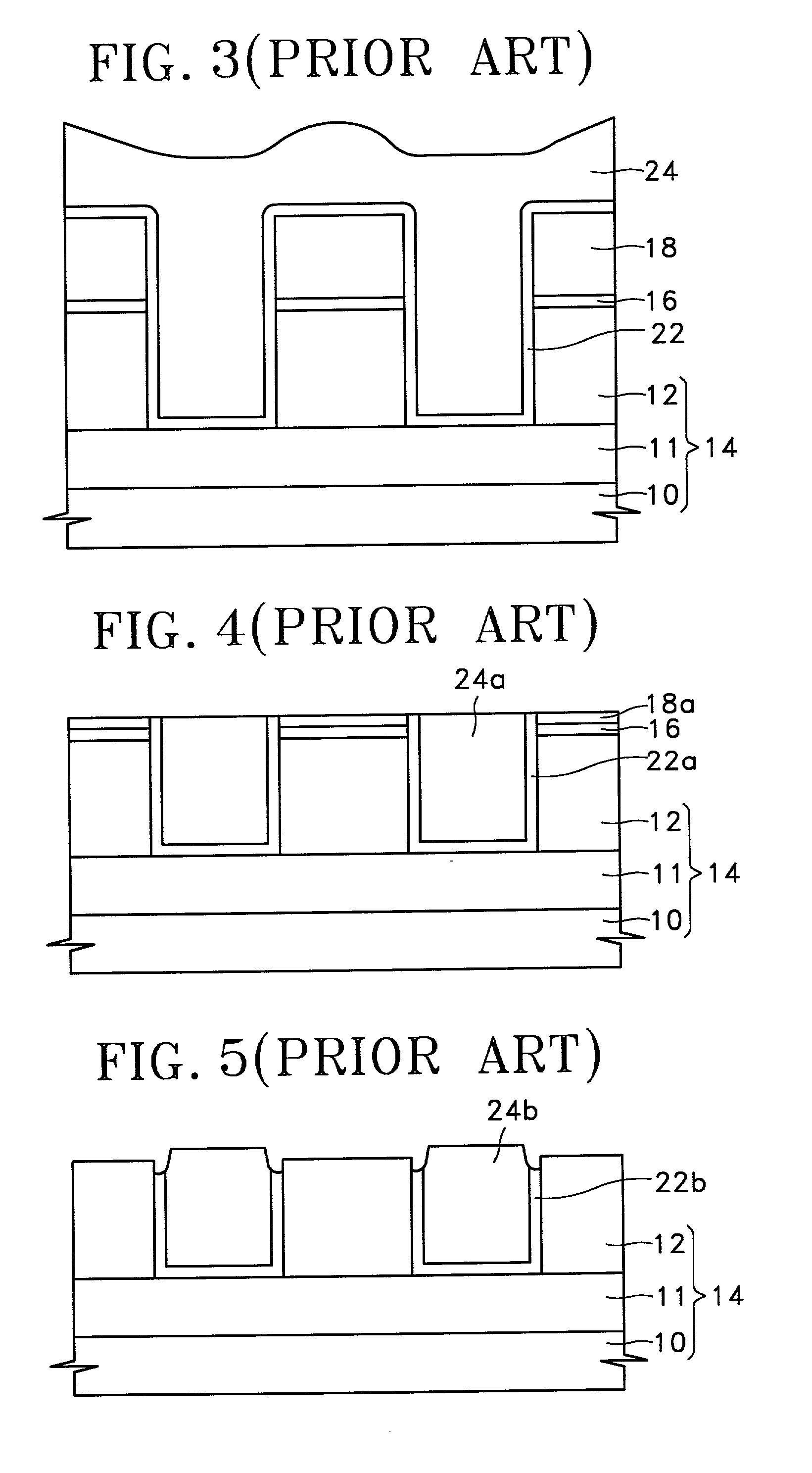
[0033] Subsequently, the hard mask layer and the pad oxide layer are pat...
embodiment 2
[0041] FIGS. 15 and 16 show the key steps in another embodiment of a method of manufacturing a trench isolation layer according to the present invention. Referring to FIG. 15, a pad oxide layer and a hard mask layer are sequentially deposited over a semiconductor substrate 204 and patterned to form a hard mask pattern 208 and a pad oxide pattern 206, and to expose a portion of the upper surface of the semiconductor substrate. Next, a spacer 210 is formed along the sidewalls of the hard mask pattern 208 and a pad oxide pattern 206. As in the first embodiment, the spacer 210 does not need to be formed at this stage of the process.
[0042] Subsequently, a thermal oxide layer 212 is formed on the exposed portion of the upper surface of the semiconductor substrate 204. That is, the portion of the semiconductor substrate 204 at which the isolation layer will be formed is subjected to thermal oxidation. Hence, an oxide layer grows from the exposed surface of the semiconductor substrate 204, ...
PUM
 Abstract
Description
Claims
Application Information
 - R&D
- Intellectual Property
- Life Sciences
- Materials
- Tech Scout
- Unparalleled Data Quality
- Higher Quality Content
- 60% Fewer Hallucinations
Browse by: Latest US Patents, China's latest patents, Technical Efficacy Thesaurus, Application Domain, Technology Topic, Popular Technical Reports.
© 2025 PatSnap. All rights reserved.Legal|Privacy policy|Modern Slavery Act Transparency Statement|Sitemap|About US| Contact US: help@patsnap.com