Method for manufacturing an interconnect structure for stacked semiconductor device

a technology of interconnect structure and semiconductor, which is applied in the direction of semiconductor devices, semiconductor/solid-state device details, electrical apparatus, etc., can solve the problems of loss of planar smoothness, the surface of multi-layer film becomes increasingly irregular, and the above-mentioned structure cannot be directly used

Inactive Publication Date: 2002-06-20
LAPIS SEMICON CO LTD +1
View PDF0 Cites 107 Cited by
  • Summary
  • Abstract
  • Description
  • Claims
  • Application Information

AI Technical Summary

Benefits of technology

[0015] By this technique, that is by forming a grounding layer between the two substrates, the radiation noise generated from respective elements on the semiconductor substrate are absorbed by the grounding layer, whilst the radiation noise generated from each element on the opposite side semiconductor substrate is similarly absorbed by the grounding layer, so that it is possible for the grounding layer to eliminate the reciprocal effect on the semiconductor elements on the semiconductor substrates. Since a common grounding layer is provided between the two substrates, it is possible to effect three-dimensional grounding interconnection via the opening to reduce the grounding wiring length.
[0018] Since the grounding layer and the power source layer operating for grounding and as a power source of the respective elements of the two substrates are provided between the substrates, the wiring length can be effectively reduced, whilst the radiation noise generated from one of the semiconductor substrates can be absorbed by the grounding layer.
[0019] The present invention thus provides an arrangement in which the grounding layer and the power source layer are sandwiched between the two substrates when the substrates are bonded together. Thus, there are provided means for reducing the wiring and prohibiting reciprocal interference of the radiation noises from both substrates.
[0021] If a conductor layer serving as a power source layer is provided on each of the first and second substrates for extending parallel to a conductor layer operating as a grounding layer, these conductor layers can serve as power sources for the first and second substrates via the through-holes, thus improving the efficiency.
[0022] Also, in the manufacturing method according to the present invention, the first and second substrates from the separate processes, carrying the semiconductor elements, are bonded together by the solid state bonding technique. Thus, the multilayer substrates, comprised of semiconductor substrates having different functions, can be produced easily, thus assuring efficient manufacture.

Problems solved by technology

However, if the radiation noise on the multi-layer semiconductor substrate is to be prohibited from occurring, the above-mentioned structure cannot directly be used.
With the increasing number of layers of the multi-layer film, the surface of the multi-layer film becomes increasingly irregular such that planar smoothness is lost.
If the number of layers is increased further, the film surface becomes increasingly irregular to cause line breakage in the course of the process.
Thus, mere contact is insufficient to produce the connection.

Method used


Image

  • Method for manufacturing an interconnect structure for stacked semiconductor device
  • Method for manufacturing an interconnect structure for stacked semiconductor device
  • Method for manufacturing an interconnect structure for stacked semiconductor device

Examples


Embodiment Construction

of the Manufacturing Process

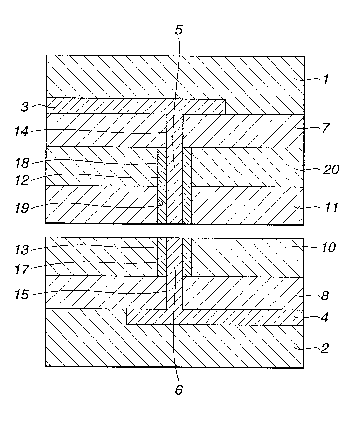
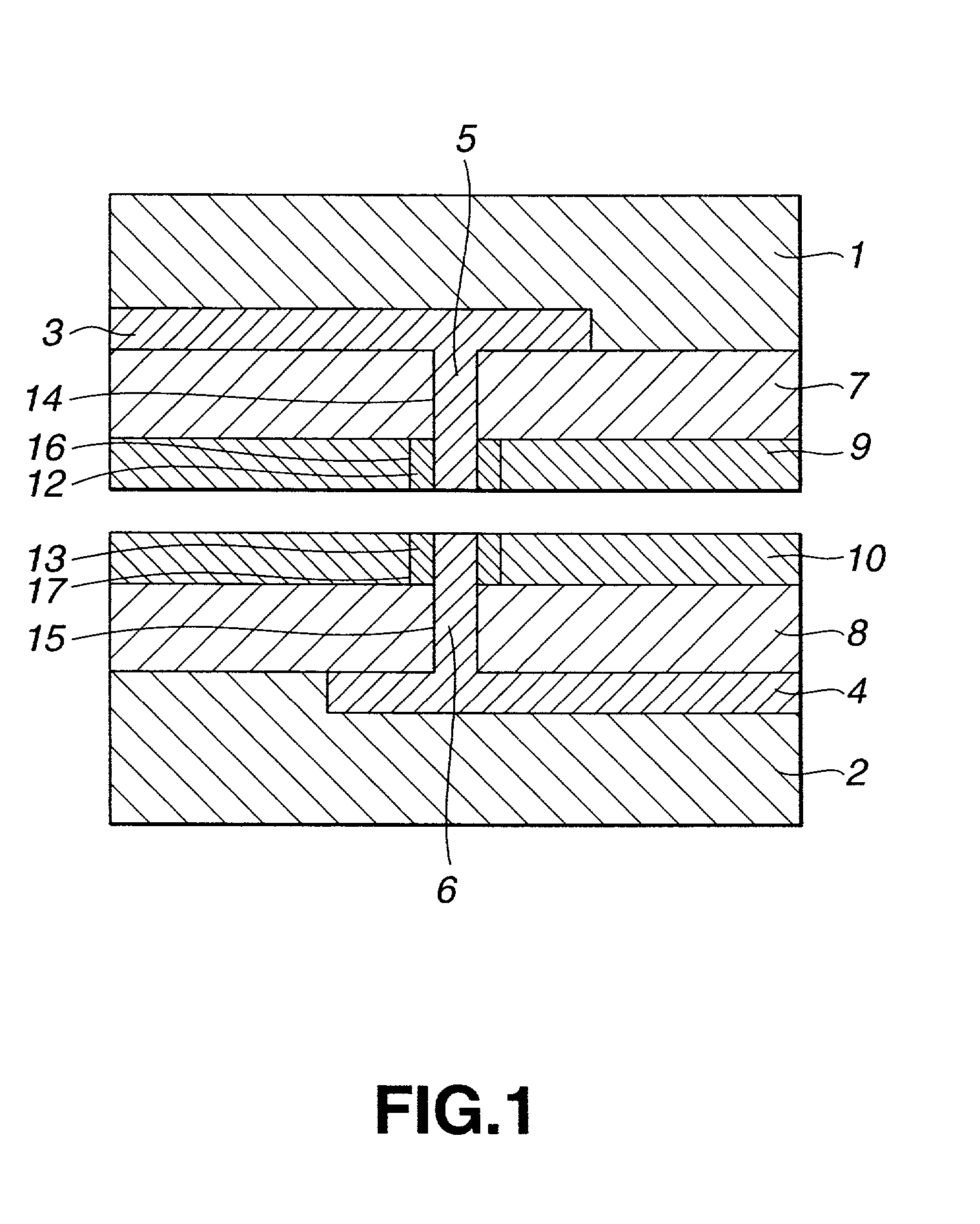
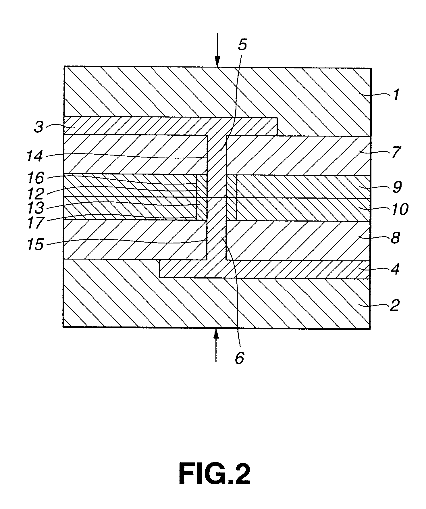
[0092] In the present embodiment, two semiconductor substrates, each carrying semiconductor elements, are connected to each other by the following process steps:

[0093] (1) a step of previously taking out a wiring electrode on a first semiconductor substrate;

[0094] (2) a step of sequentially depositing an insulating layer and a grounding layer on the first substrate and boring through-holes connecting to the wiring electrode in the insulating layer and the grounding layer;

[0095] (3) a step of forming a through-hole wiring in the through-holes for electrical connection to the wiring electrode;

[0096] (4) a step of forming an insulating layer in the through-hole wiring in the grounding layer between the through-hole wiring and the grounding layer;

[0097] (5) a step of smoothing one of the major surfaces of the substrate;

[0098] (6) a step of previously taking out a wiring electrode on a second semiconductor substrate;

[0099] (7) a step of sequentially depositing...


PUM


Abstract

In a multi-layer interconnection structure, the wiring length is to be reduced, and the interconnection is to be straightened, at the same time as measures need to be taken against radiation noise. To this end, there is disclosed a semiconductor device in which plural semiconductor substrates, each carrying semiconductor elements, are bonded together. On each semiconductor substrate is deposited an insulating layer through which is formed a connection wiring passed through the insulating layer so as to be connected to the interconnection layer of the semiconductor element. On a junction surface of at least one of the semiconductor substrates is formed an electrically conductive layer of an electrically conductive material in which an opening is bored in association with the connection wiring. The semiconductor substrates are bonded together by the solid state bonding technique to interconnect the connection wirings formed on each semiconductor substrate.

Description

[0001] 1. Field of the Invention[0002] This invention relates to a semiconductor device in which layered films and wiring layers on a semiconductor substrate are bonded together using the solid state bonding technique, and a manufacturing method therefor. More particularly, it relates to an improvement intended for reducing radiation noises.[0003] 2. Description of the Prior Art[0004] In the filed of semiconductor devices, there has so far been known a electromagnetic noise shield for eliminating the noise in which an electrically conductive material is applied to the perimeter of a wiring layer on a semiconductor substrate in an encapsulating fashion, as disclosed for example in Japanese Laying-Open Patent H-5-47767.[0005] There is also known from the Japanese Laying-Open Patent H-5-47943 such a structure in an analog / digital hybrid semiconductor device in which a shield line is arranged between a high-frequency digital signal line and an analog signal line susceptible to noise, at...

Claims


Application Information

Patent Timeline
Patent Type & Authority Applications(United States)
IPC IPC(8): H01L27/04H01L21/02H01L21/3205H01L21/768H01L23/52H01L23/552H01L23/58H01L27/00
CPCH01L21/768H01L24/80H01L23/585H01L25/0657H01L25/50H01L2224/48091H01L2224/48463H01L2225/06513H01L2225/06541H01L2924/01013H01L2924/01029H01L2924/01079H01L2924/14H01L2924/3025H01L23/552H01L2224/80896H01L2224/80895H01L2224/80357H01L2924/01068H01L2924/01067H01L24/48H01L2924/00014H01L2224/05547H01L2224/05599H01L2224/85399H01L2224/02126H01L2224/80986H01L2224/02125H01L2224/08145H01L2224/45099H01L2224/45015H01L2924/207H01L27/04
Inventor SUGA
Owner LAPIS SEMICON CO LTD
Why Eureka
Try Eureka