Contact between element to be driven and thin film transistor for supplying power to element to be driven

a technology of thin film transistor and contact between elements, which is applied in the direction of luminescent display devices, identification means, instruments, etc., can solve the problems of uneven grain size of polycrystalline silicon, on-current characteristic or the like of tft, and other problems

Inactive Publication Date: 2002-07-04
SANYO ELECTRIC CO LTD
View PDF0 Cites 45 Cited by
  • Summary
  • Abstract
  • Description
  • Claims
  • Application Information

AI Technical Summary

Benefits of technology

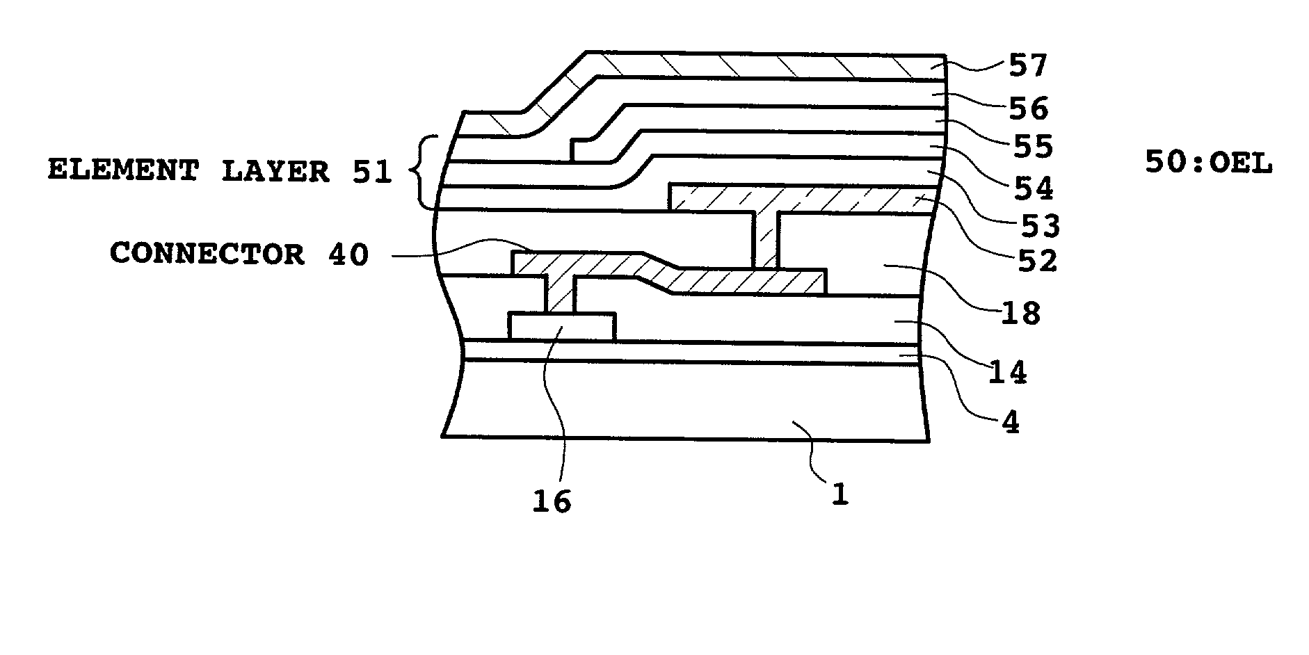
[0013] By placing the contact position between the wiring layer and the thin film transistor distant from the contact position between the wiring layer and the element to be driven, the formation of the element to be driven, which in many cases is formed at a layer above the wiring layer, on a more flat surface is facilitated. The thin film transistor and the wiring layer are separated by an insulation layer and the contact between the thin film transistor and the wiring layer is achieved through a contact hole formed on the insulation layer. The connection between the wiring layer and the element to be driven is achieved through a contact hole formed on another insulation layer for insulating the wiring layer and the element to be driven. Therefore, when the contact hole for connecting the thin film transistor and the wiring layer is formed to overlap to the position of the contact hole for connecting the wiring layer and the element to be driven, the element to be driven, which is formed at the uppermost layer, would be formed on top of an uneven surface with a large height difference due to two (steps of) contact holes. When an emissive element, for example, an organic EL element which uses an organic compound in the emissive layer, is used as the element to be driven, electric field concentration or the like tends to occur at the layer which includes the organic compound if the flatness of the formation surface is not good, and a dark spot which cannot illuminate tends to be generated from such electric field concentration. Therefore, by placing at a distance the contact between the wiring layer and the element to be driven from the contact between the thin film transistor and the wiring layer, the flatness of the formation region of the element to be driven can be improved.
[0015] By covering the contact hole region of the first electrode by a flattening layer, that is, by filling the recessed section caused by the presence of the contract hole by the flattening layer, a surface which has a very high flatness can be obtained by the first electrode and the flattening layer. Thus, by forming the emissive element layer on the surface with very high flatness, the reliability of the element can be improved.
[0017] An emissive element layer is formed above the first electrode, but, because the recess section on the first electrode generated by the presence of the contact hole is covered by a flattening layer, the first electrode and the flattening layer can create a very flat surface even when the recess section is deep such that the reliability of the element can be improved by forming the emissive element layer on top of the surface with a high flatness.
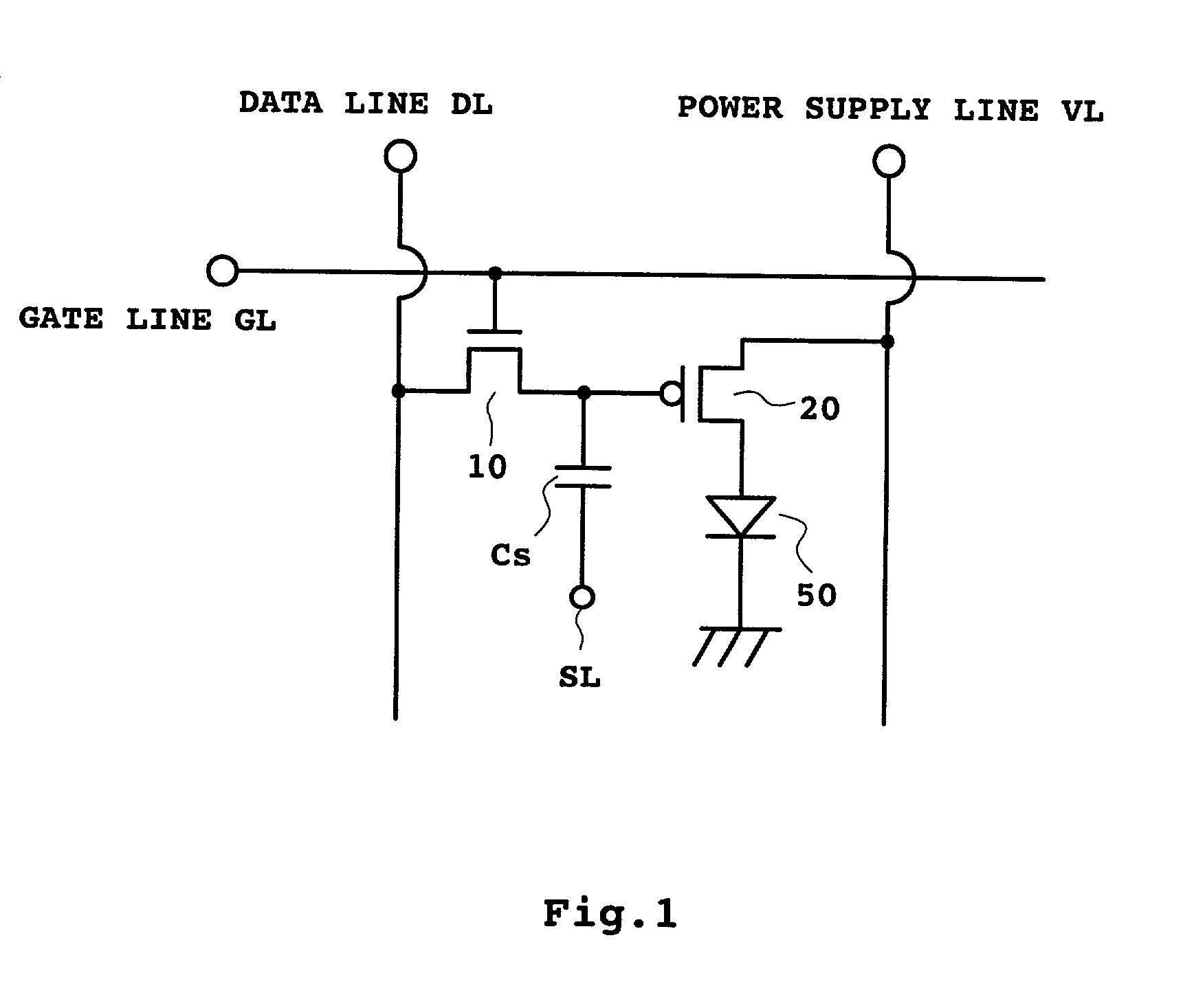
[0018] According to another aspect of the present invention, it is preferable that the element to be driven is an organic electroluminescence element which employs an organic compound as an emissive layer. Although such an organic EL element has high brightness and wider selection ranges for the illumination color and material, because the organic EL element is current driven, variation in the amount of supplied current causes a variation in the illumination brightness. By using the circuit structure of the pixel or placement as described above, it is possible to easily maintain uniformity of the supplied current. In addition, by employing the placement and structure of the contact points as described above, the aperture ratio can be increased and the element layer such as the emissive layer can be formed on a flat surface, and a more reliable element can be obtained.

Problems solved by technology

Because of various reasons such as, for example, energy variation in the irradiating laser at the irradiation surface, the grain size of the polycrystalline silicon is not uniform.
When grain size is not uniform, in particular around the TFT channel, there is a problem in that the on-current characteristic or the like of the TFT may also vary.

Method used


Image

  • Contact between element to be driven and thin film transistor for supplying power to element to be driven
  • Contact between element to be driven and thin film transistor for supplying power to element to be driven
  • Contact between element to be driven and thin film transistor for supplying power to element to be driven

Examples


first embodiment

[0040] First Embodiment

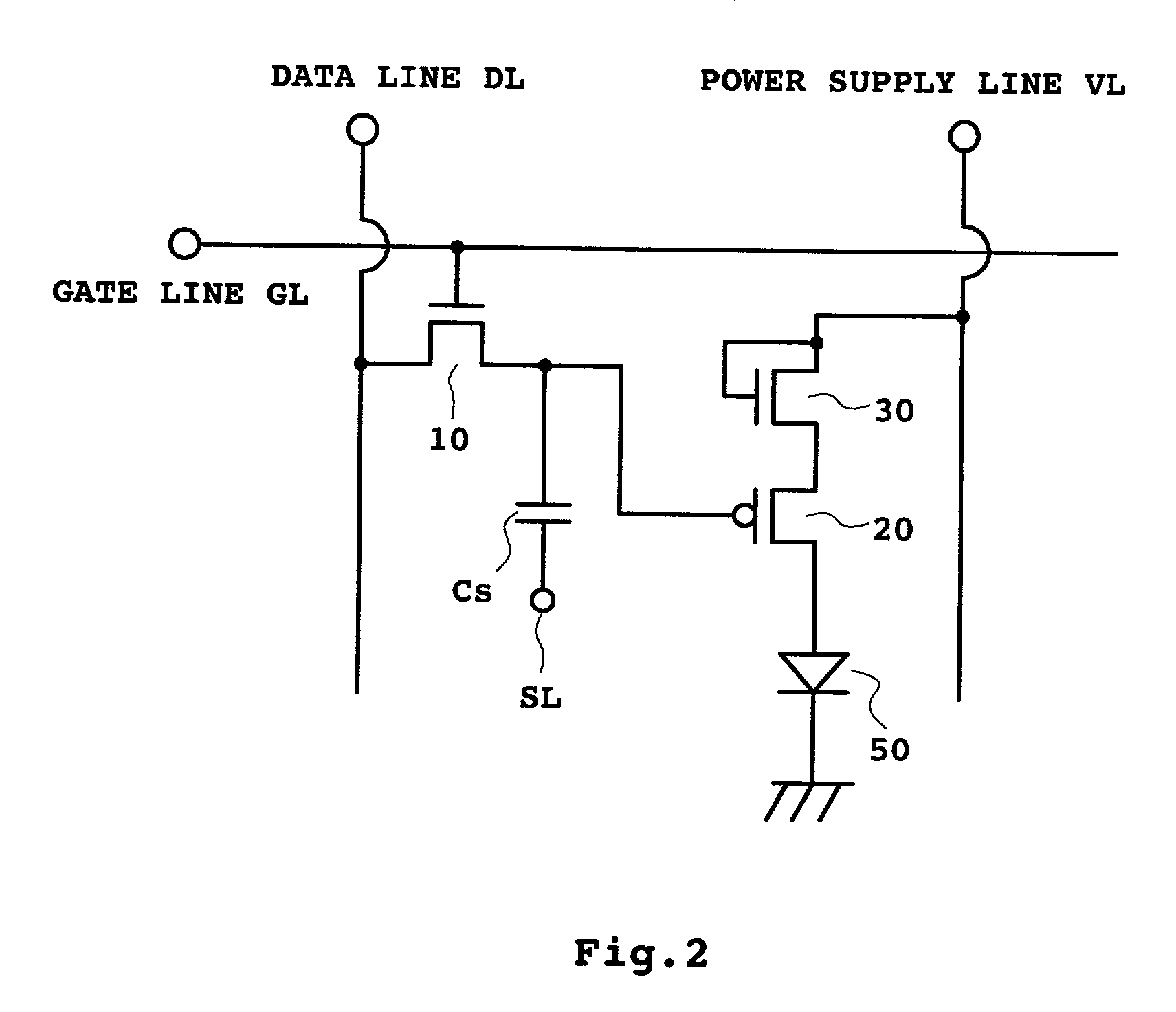
[0041] FIG. 2 shows a circuit structure of one pixel in an active matrix type EL display device having m rows and n columns according to a first embodiment of the present invention. As shown in FIG. 2, each pixel comprises an organic EL element 50, a switching TFT (first TFT) 10, an element driving TFT (second TFT) 20, and an storage capacitor Cs, and is constructed in a region surrounded by a gate line GL extending in the row direction and a data line DL extending in the column direction. In the first embodiment, a compensation TFT 30 having the conductive characteristic opposite of that of the second TFT 20 is provided between the power supply line VL and the second TFT 20. The gate and either the source or the drain of the compensation TFT 30 are connected to provide a diode connection. The diode is connected in the forward direction between the power supply line VL and the second TFT 20. Thus, the compensation TFT can be operated without supplying any desi...

second embodiment

[0071] Second Embodiment

[0072] A second embodiment of the present invention will now be described. In the first embodiment, in order to prevent variation in the illumination brightness among pixels as a result of characteristic variations in the transistor, a compensation thin film transistor having an opposite conductive characteristic as the element driving thin film transistor is provided. In contrast, in the second embodiment, the variation in the illumination brightness among pixels is inhibited by considering the placement of the element driving thin film transistor (second TFT). FIGS. 10A and 10B show an example configuration of one pixel according to the second embodiment. FIG. 10A is a schematic planer view and FIG. 10B is a cross sectional view along the B-B line in FIG. 10A. This structure is shown with the same circuit structure as that of FIG. 1. In these figures, the components corresponding to those in the drawings that are already explained will be referred to by the...

third embodiment

[0090] Third Embodiment

[0091] A method for efficiently connecting a plurality of second TFTs 20 and corresponding organic EL element 50 within one pixel will now be described as a third embodiment of the present invention. As described in the first embodiment and as shown in FIG. 11 of the second embodiment, provision of a plurality of second TFTs 20 between an organic EL element 50 and a power supply line VL within one pixel is advantageous from the viewpoint of improvements in reliability, characteristic, or the like. In a case wherein a plurality of second TFTs 20 are provided within one pixel, as shown in FIG. 11, by respectively connecting the second TFTs 20a and 20b and the organic EL element 50, a current can more reliably be supplied from the power supply line VL to the organic EL element 50 via the second TFTs 20. However, in an organic EL element of the type shown in FIG. 10B in which light from the emissive layer 55 is emitted from a transparent anode 52 to the outside vi...


PUM


Abstract

A TFT (20) for controlling the power supplied to an element to be driven (50), such as an organic EL element which operates based on the supplied power, is provided between the element to be driven (50) and a power supply line VL. The TFT (20) and the element to be driven (50) are electrically connected by a wiring layer (40). The contact position between the wiring layer (40) and the TFT (20) and the contact position between the wiring layer (40) and the element to be driven (50) are positioned so as to be distant from each other. Alternatively, at least the contact hole region of a first electrode (52) of the element (50) is covered by a flattening layer. With this structure, it is possible to realize a flatter surface on which to form, for example, the emissive layer of the element to be driven.

Description

[0001] 1. Field of the Invention[0002] The present invention relates to an electroluminescent display device, and in particular, to transistors constructing the circuit structure in the pixel section of an electroluminescent display device.[0003] 2. Description of the Related Art[0004] An electroluminescence (hereinafter referred to as EL) display device which uses an EL element which is a self-illuminating element as an illumination element in each pixel has attracted a strong interest as an alternative display device for a display device such as a liquid crystal display device (LCD) and a CRT because the EL display device has advantages such as thin width and low power consumption, in addition to the advantage of being self-illuminating. Such an EL display device has thus been researched.[0005] In particular, there is a high expectation for an active matrix type EL display device in which a switching element such as, for example, a thin film transistor for individually controlling...

Claims


Application Information

Patent Timeline
Patent Type & Authority Applications(United States)
IPC IPC(8): G09F9/30H01L51/50G09G3/20G09G3/30G09G3/32H01L21/20H01L21/336H01L27/08H01L27/32H01L29/786H05B33/00
CPCG02F1/13624G09G3/3233G09G2300/0417G09G2300/0426G09G2300/0465G09G2300/0809G09G2300/0842G09G2300/0885G09G2320/0204G09G2320/0233G09G2320/043G09G2330/021H01L27/3244H01L27/3248H01L27/3262H10K59/123H10K59/1213H10K59/12G09G3/30H05B33/00
Inventor ANZAI, KATSUYA
Owner SANYO ELECTRIC CO LTD
Why Eureka
Try Eureka