Low cost optical bench having high thermal conductivity

a technology of optical bench and thermal conductivity, which is applied in the direction of optical elements, semiconductor lasers, instruments, etc., can solve the problems of poor thermal conductivity of the base plate, high cost of package fabrication, and inability to properly heat dissipate over the tec top surface, etc., to achieve excellent heat dissipation properties, facilitate laser welding operations, and high thermal conductivity

Inactive Publication Date: 2002-07-04
CORNING OTI SPA
View PDF3 Cites 26 Cited by
  • Summary
  • Abstract
  • Description
  • Claims
  • Application Information

AI Technical Summary

Benefits of technology

0018] Preferably, the substrate is made of a material with high thermal conductivity. More preferably, the substrate is made of a ceramic material, such as an AlN based material. The optical bench according to the present

Problems solved by technology

As the optical bench needs to be placed on a TEC, Applicants have observed that using a material with poor thermal conductivity, such as Kovar, for the baseplate does not allow proper heat dissipation over the TEC top surface.
Manufacture of packages with ceramic terminal feed-through for pin-out, as that described in FIG. 2, adds high costs to package fabrication, especially if compared to the seal-around technology.
In this way, heat di

Method used


Image

  • Low cost optical bench having high thermal conductivity
  • Low cost optical bench having high thermal conductivity
  • Low cost optical bench having high thermal conductivity

Examples


first embodiment

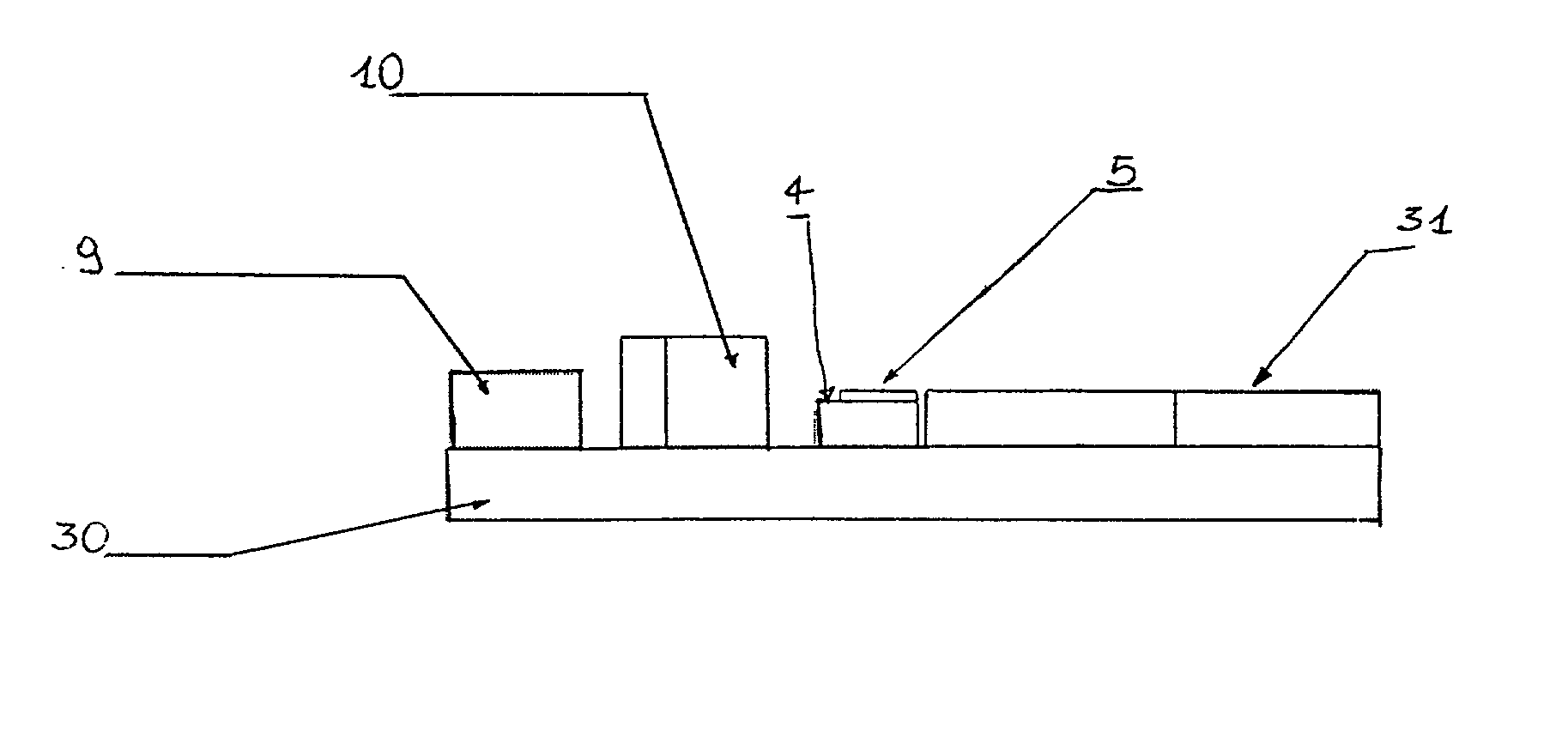
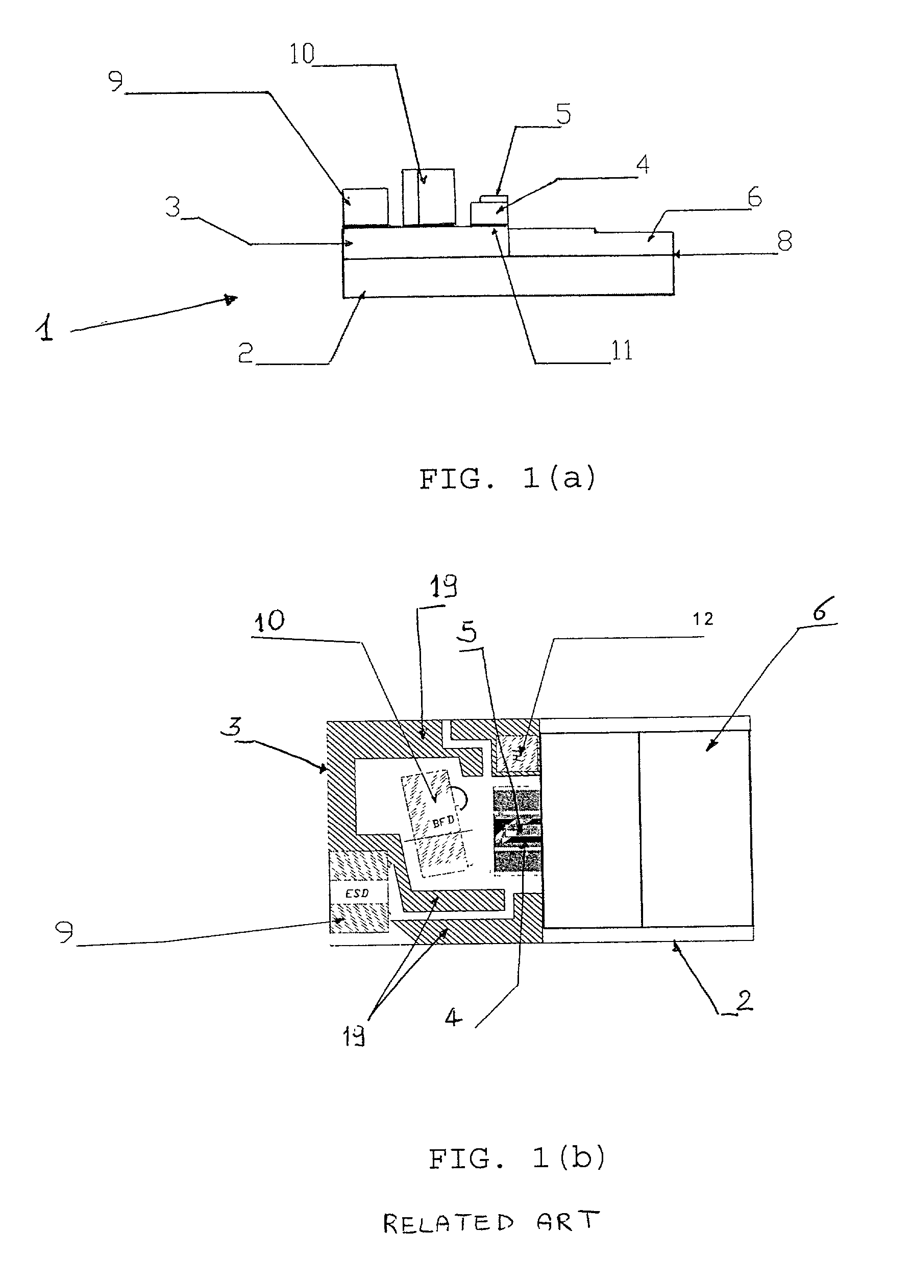
[0046] The optical bench according to the present invention is shown in FIG. 3. The optical bench comprises a single insulating baseplate or substrate 30. Welding platform 31, heat-sink 4 with laser unit 5 (laser diode or laser diode chip) and complementary internal devices, such as ESD 9, back-field detector 10 and thermistor 12, are mounted directly on top of the ceramic baseplate 30. Complementary internal devices can be bonded to the ceramic baseplate by the use of solder or by co-firing. FIG. 3(b) illustrates a top view of the baseplate 30. The dotted-dashed line 33 indicates the optical axis of baseplate. The laser is aligned so that its light emission is directed substantially along the optical axis of the baseplate. Peripheral metallised tracks 32 extend over at least part of the baseplate surface in a direction substantially parallel to the optical axis 33. Metallised tracks or circuit patterns 32 can be made for instance by the techniques of thin film (lithography) or of t...

second embodiment

[0056] We have described the preferred modes of carrying out the invention. An alternative solution to the problem of having a correct pin-out in low-cost packages, could be to have a two-substrate structure, in particular an insulating U-shaped circuit board mounted on a rigid baseplate. This second embodiment is shown in FIG. 5. A rigid U-shaped circuit board 50 of an insulating material is mounted on a baseplate 52, e.g., bonded to the baseplate by high-temperature solder 53. Co-firing can be used instead of soldering for bonding the circuit board to the baseplate. Both substrates can be made of a material of high thermal conductivity such as an AlN based material. The baseplate 52 can be made also of a metallic material having high thermal conductivity, such as Cu--W alloy. The U-shaped legs of the circuit board 50 project in the longitudinal direction of the baseplate, i.e., in a direction substantially parallel to the optical axis 54. U-shaped legs are provided with metallised...

third embodiment

[0057] Another two-substrate solution could be the use of conductive vias through an insulating circuit board, which is provided with circuit patterns and through-holes and which is placed on an insulating baseplate. This third embodiment of the present invention is shown in FIG. 6. FIG. 6(a) shows the top view of the optical bench. A circuit board 60 provided with circuit patterns 64 and metallised through-holes 63 [indicated in FIGS. 6(a) and 6(b) as 63a to 63d] is bonded to a rigid baseplate 61. Peripheral metallised tracks 62 [indicated in FIGS. 6(a) and 6(c) as 62a to 62d] are present on the top surface of the baseplate 61 and extend along a region of baseplate 61 on a side of a fixing region, shown as hatched in FIG. 6(a), reserved for mounting a welding platform. Preferably, circuit board 60 and baseplate 61 are made of AlN based materials. Through-holes 63 in the circuit board act as conductive vias to electrically connect the circuit patterns 64 on the top surface of the ci...


PUM


Abstract

The invention relates with an optical bench for optoelectronic packages comprising a rigid insulating substrate, the substrate having a top surface along which it is defined an optical axis, the substrate comprising: a device region for mounting at least an optoelectronic device in alignment with the optical axis, and a fixing region adjacent to the device region for affixing at least an optical component in alignment with the optical axis. The substrate further comprises a third region provided with metallised tracks, the third region extending over the substrate top surface along at least part of one side of the fixing region in a direction substantially parallel to the optical axis. The invention also relates with an optical bench comprising: a single baseplate having a device region and a fixing region; a welding platform mounted directly on said fixing region; a heat sink mounted directly on said device region; and an optoelectronic device directly mounted on said heat sink.

Description

[0001] This application claims the benefit of European Application 00128596.41 filed Dec. 28, 2000 and U.S. Provisional Application 60 / 259,206 filed Jan. 3, 2001.BACKGROUND OF THE INVENTION[0002] 1. Field of the Invention[0003] The invention relates to an optical bench and to an optoelectronic package for housing at least an active optoelectronic device and its associated electronic circuit elements. In particular, the invention concerns a low cost thermally controlled optoelectronic package.[0004] 2. Related Art[0005] In high-power laser devices, the laser unit, laser diode or laser diode chip, is generally mounted on a heat-sink made of a material with high thermal conductivity, such as diamond, SiC or AlN, for thermal dissipation during operation of the laser. The heat-sink is bonded onto a circuit board, which can accommodate all or part of the complementary internal devices of the laser package, such as a thermistor, a back-field photodetector and circuit patterns. Optical comp...

Claims


Application Information

Patent Timeline
IPC IPC(8): G02B6/42H01S5/02H01S5/022H01S5/024
CPCG02B6/4201G02B6/4202G02B6/4237H01S5/02476H01S5/02248H01S5/02415H01S5/02216H01S5/02325
Inventor SHAW, MARK A.
Owner CORNING OTI SPA
Why Eureka
Try Eureka