

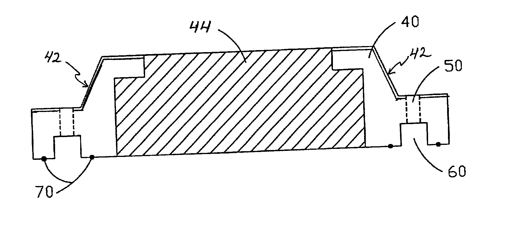
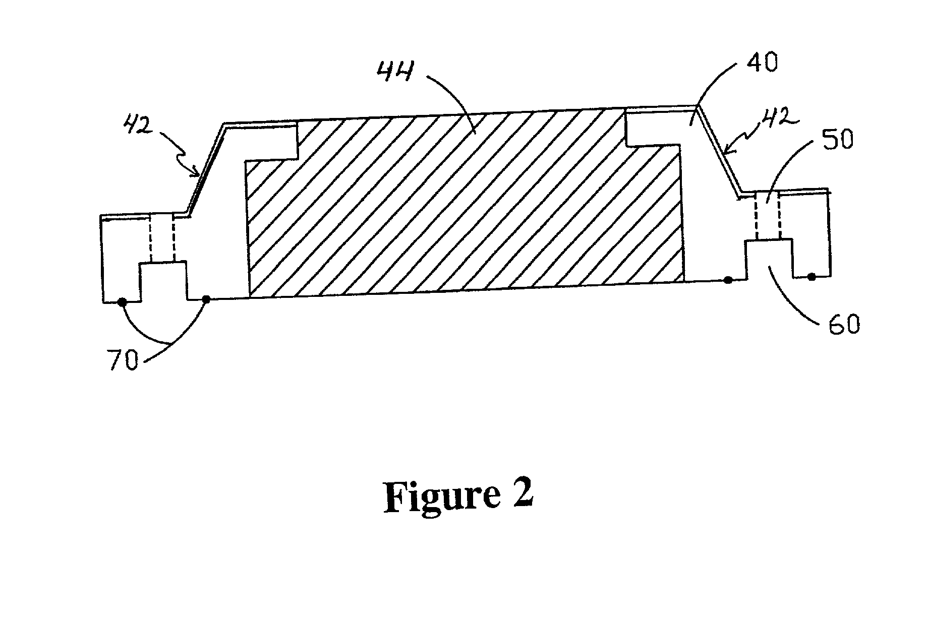
Corrosion resistant component of semiconductor processing equipment and method of manufacture thereof
a technology of processing equipment and components, which is applied in the field of high density plasma etching chambers, can solve the problems of reducing the physical size of the components of the equipment, cracking of the coating, and affecting the performance of the equipmen
- Summary
- Abstract
- Description
- Claims
- Application Information
AI Technical Summary
Problems solved by technology
Method used
Image

Examples
Embodiment Construction
[0018] The first layer of conductive material in an integrated circuit (IC) is a thin film of polysilicon or polysilicide that is in direct contact with transistors embedded in the wafer surface. After the polysilicon has been etched, only the conductive traces needed to operate the transistors and make point-to-point connections between them remain. Because the poly etch is conducted on the wafer surface, control of contamination is particularly important.
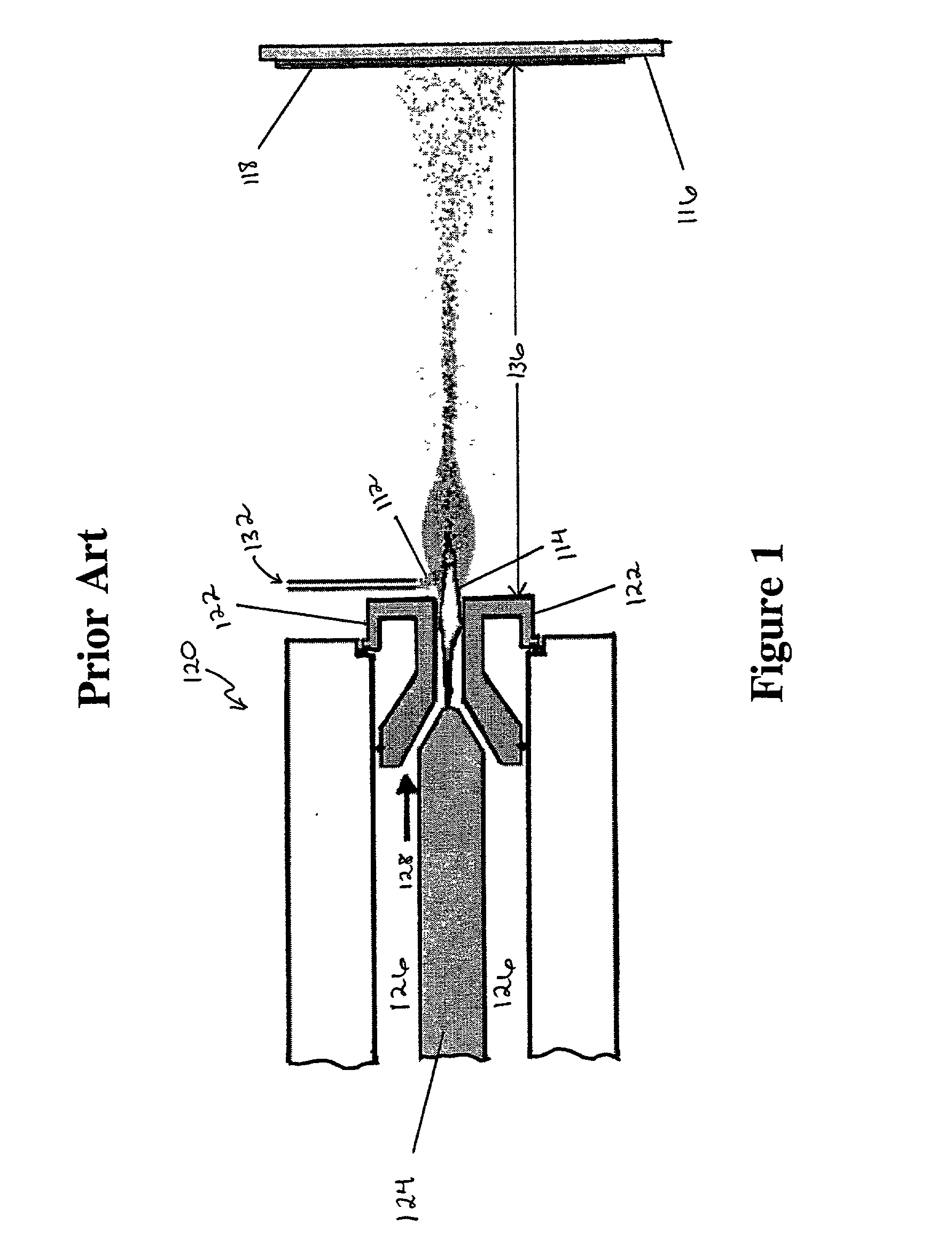
[0019] Typically, a processing chamber that is used for etching materials such as polysilicon requires relatively high energies to achieve the desired etch result. The need for high energies stems from the need to bombard and break the strong bonds of the polysilicon films and drive chemical reactions to form volatile etch products. These chambers are therefore referred to as "high density etch chambers," that are capable of producing high plasma densities in order to provide a high ion flux to the wafer and achieve high etch rate...
PUM
| Property | Measurement | Unit |
|---|---|---|
| Density | aaaaa | aaaaa |
| Energy | aaaaa | aaaaa |
Abstract
Description
Claims
Application Information