Method for manufacturing tantalum oxy nitride capacitors

Inactive Publication Date: 2002-07-25
SK HYNIX INC
View PDF5 Cites 8 Cited by
  • Summary
  • Abstract
  • Description
  • Claims
  • Application Information

AI Technical Summary

Benefits of technology

0014] Therefore, a method for manufacturing a tantalum oxy nitride capacitor is disclosed which reduces a number of steps and increases yield by performing the step of doping a MPS (Metastable Poly Silicon) in the same chamber in-situ with the forming of a nitride film before the forming of a tantalum o

Problems solved by technology

However, there is a limit to the size needed for storing charge for satisfying a required capacitance.
Thus, there occurs a difficulty in miniaturizing the capacitor.
Due to the increase in temperature caused by the plasma, a problem occurs in that a tantalum oxy nitride film deposited by the low pressure chemical vapor deposition (LPCVD) is deposited non-uniformly in the wafer and thus it is difficult to meet process requirements.
Particularly, it is necessary that the tantalum oxy nitride film b

Method used


Image

  • Method for manufacturing tantalum oxy nitride capacitors
  • Method for manufacturing tantalum oxy nitride capacitors
  • Method for manufacturing tantalum oxy nitride capacitors

Examples


Example

[0033] A preferred embodiment will now be described with reference to the accompanying drawings. But it is understood that the disclosure is not to be limited to this embodiment.

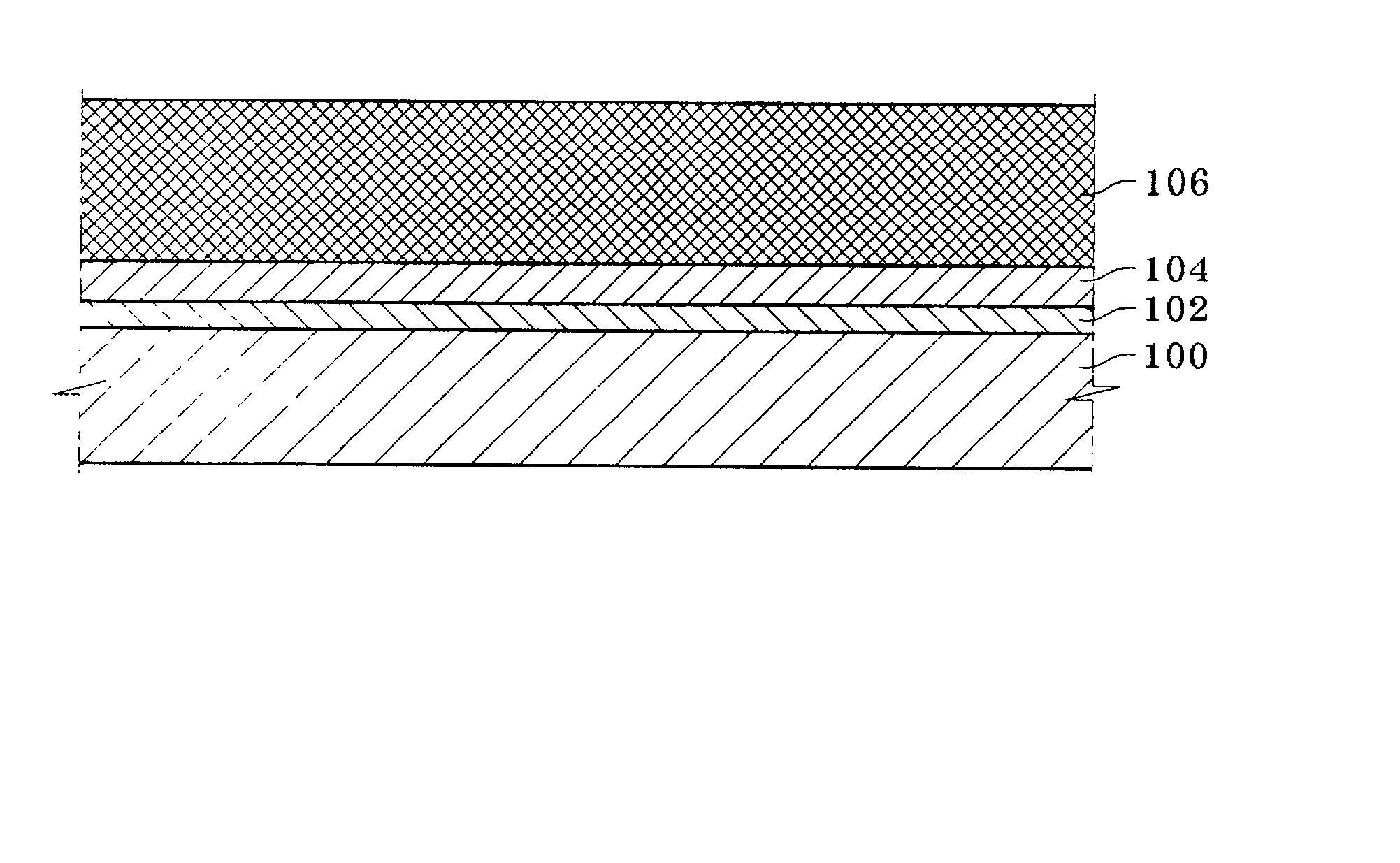
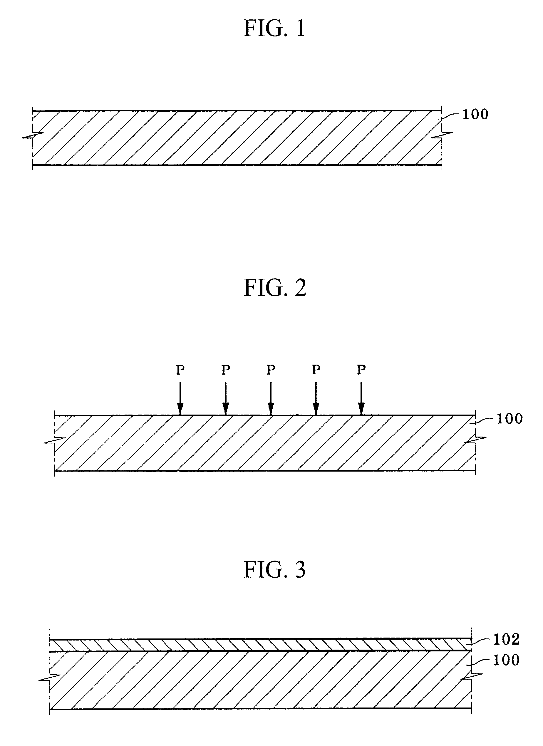
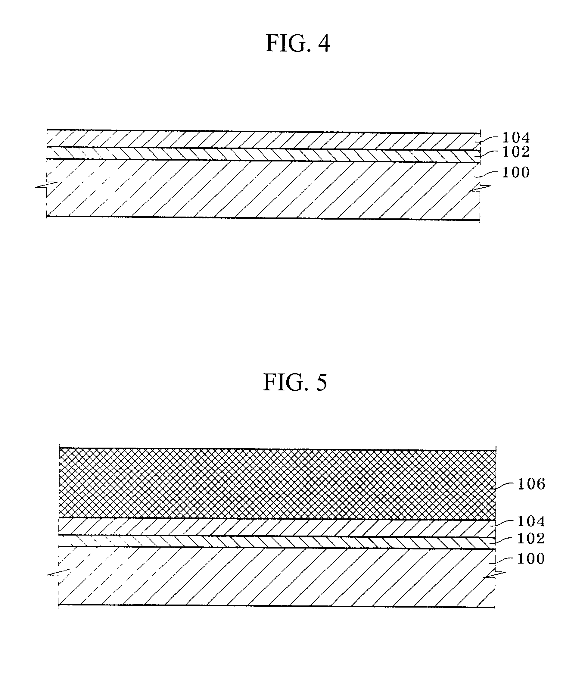
[0034] FIGS. 1 through 5 are views illustrating the sequence of processes for manufacturing a tantalum oxy nitride capacitor.

[0035] In the process according to the disclosure, as illustrated in FIG. 1, a lower electrode 100 is formed on the surface of a semiconductor substrate 10. At this time, the lower electrode is selected from undoped silicon, low doping silicon or doped / undoped silicon which are capable of MPS growth. At this time, a thin film used as the electrode is an amorphous silicon film deposited at a temperature of below about 560.degree. C. by using a gas containing a silicon source such as SiH.sub.4, Si.sub.2H.sub.6, SiH.sub.2Cl.sub.2 and the like and a gas containing PH.sub.3 such as PH.sub.3 / N.sub.2, PH.sub.3 / He, PH.sub.3 / SiH.sub.4, PH.sub.3 / Ar and the like. At this time, conditions such as ...


PUM

PropertyMeasurementUnit
Pressureaaaaaaaaaa
Angleaaaaaaaaaa
Angleaaaaaaaaaa

Abstract

A method for manufacturing a capacitor using a tantalum oxy nitride (TaON) film in a process for a semiconductor device. More particularly, a method for manufacturing a capacitor which reduces a number of steps and thus increases yield by in-situ performing P-doping after forming a MPS (Metastable Poly Silicon) on a lower electrode and forming a nitride film before forming a tantalum oxy nitride film to prevent the concentration of phosphor contained in the lower electrode from being reduced by removing the phosphor on the surface of the lower electrode in a cleaning process between the above two steps, for thereby increasing the capacitance of the capacitor.

Description

[0001] 1. Technical Field[0002] A method for manufacturing a capacitor with a tantalum oxy nitride (TaON) film for a semiconductor device is disclosed. More particularly, a method for manufacturing a capacitor is disclosed with a reduced number of steps and thus an increased yield by in-situ performing the step of executing P-doping after forming a MPS (Metastable Poly Silicon) on a lower electrode and the step of forming a nitride film before forming a tantalum oxy nitride film. The disclosed method prevents the concentration of phosphor contained in the lower electrode from being reduced by removing the phosphor on the surface of the lower electrode in a cleaning process performed between the above two steps, thereby increasing the capacitance of the capacitor.[0003] 2. Description of the Related Art[0004] Generally, a capacitor stores a charge required for the operation of a semiconductor. As the semiconductor device is highly integrated, the size of a cell decreases while the ca...

Claims


Application Information

Patent Timeline
IPC IPC(8): H01L21/02H01L21/314H01G4/33H01L21/318H01L21/822H01L21/8242H01L27/04H01L27/108
CPCH01L21/3144H01L28/40Y10T29/49128Y10T29/43Y10T29/417Y10T29/435H01L21/02271H01L21/02183H10B99/00H01L21/02356H01L21/0234
Inventor PARK, DONG-SUJEON, KWANG-SEOK
Owner SK HYNIX INC
Why Eureka
Try Eureka