

Structures and methods of anti-fuse formation in SOI
a technology of structure and method, applied in the direction of semiconductor devices, semiconductor/solid-state device details, electrical apparatus, etc., can solve the problems of increasing the likelihood of malformation of some portion of the integrated circuit during manufacture, fuses and anti-fuses require significant chip space, and the placement of an increasing number of elements in a complex circuit is often difficul
- Summary
- Abstract
- Description
- Claims
- Application Information
AI Technical Summary
Benefits of technology
Problems solved by technology
Method used
Image

Examples
first embodiment
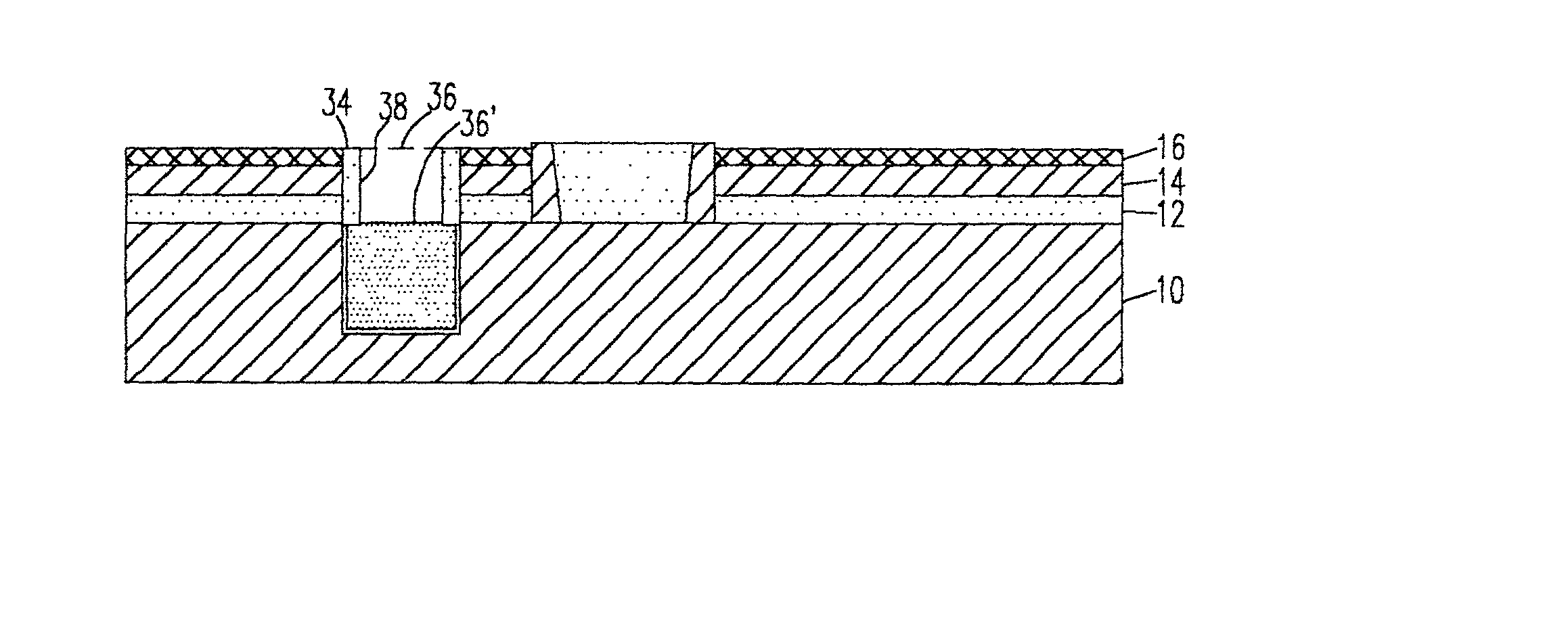
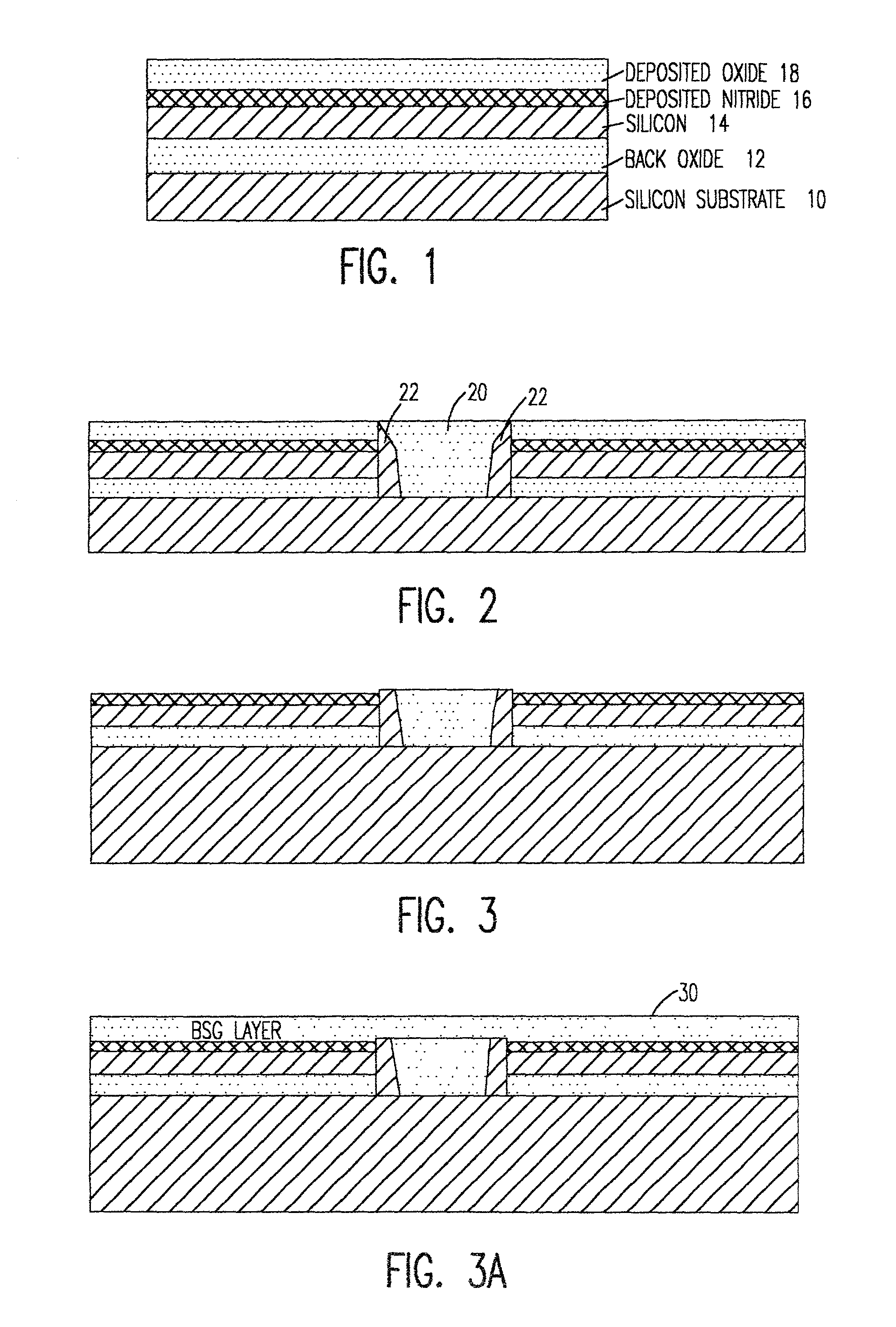
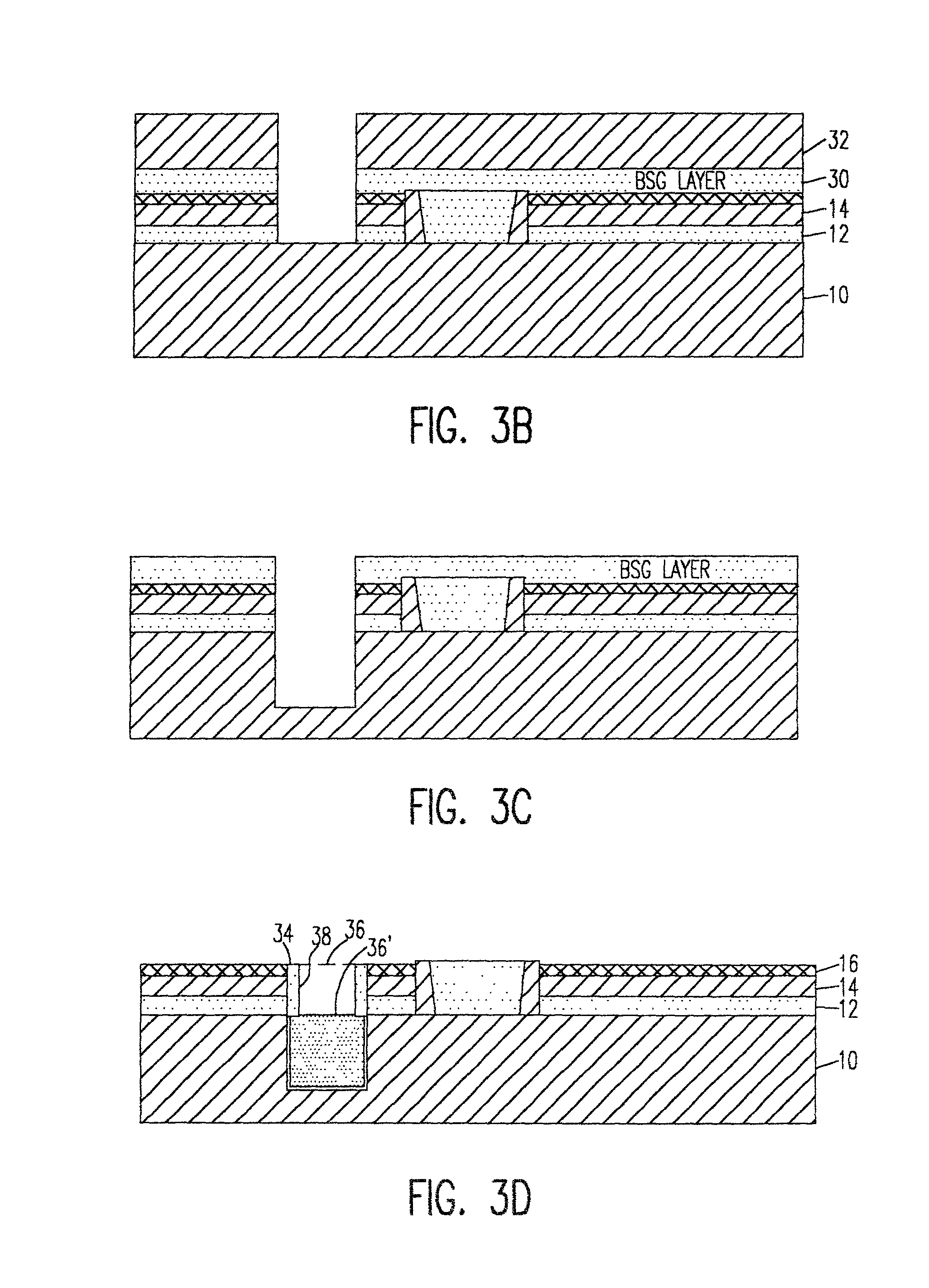
[0020] Referring now to the drawings, and more particularly to FIG. 1, there is shown, in cross-sectional view, a starting wafer for formation of an anti-fuse in accordance with the invention. As is characteristic of silicon-on-insulator (SOI) wafers, a relatively thick bulk silicon layer 10 is provided to provide mechanical robustness and facilitate handling and to provide an electrically conductive ground plane. For purposes of the practice of the invention, however, this bulk silicon is preferably formed or treated (e.g. implanted) to include dopants that regulate the bulk resistance to a desired value, as will be discussed in greater detail below. The bulk silicon is covered with an insulator 12, generally an oxide (and thus referred to as a back oxide or BOX), and the insulator is covered by a thin monocrystalline silicon layer 14 of extremely high quality, often referred to an active device layer.
[0021] It should be understood that, while the invention will be described in ter...
second embodiment
[0045] This structure may be used in several ways. If suitable isolation is provided, the capacitor 70 can be read as a two terminal device. The connection can also be used to repair, for example, bit lines or to connect redundant devices to replace marginal or inoperative devices. Further, since both electrodes of the capacitor are available, the capacitor dielectric can be damaged by an overvoltage to program the anti-fuse. Other uses and ancillary structure to accommodate them will be evident to those skilled in the art in view of the present disclosure. In any event, the connection in accordance with this second embodiment of the invention is potentially of a size which can be placed at any location in an integrated circuit including features spaced at minimum lithographic feature size and can be formed at any stage of manufacture of the integrated circuit that includes the devices or structures between which it is to be placed.
[0046] Therefore, the second embodiment of the inve...
PUM
 Abstract
Description
Claims
Application Information