Open bit line dram with ultra thin body transistors

a transistor and ultra-thin body technology, applied in the field of integrated circuits, can solve the problems of difficult formation of shallow junctions, significant problems in the conventional transistor structure, and the use of storage capacitors

Inactive Publication Date: 2002-08-15
MICRON TECH INC
View PDF0 Cites 41 Cited by
  • Summary
  • Abstract
  • Description
  • Claims
  • Application Information

AI Technical Summary

Problems solved by technology

However, other factors, such as subthreshold leakage currents and alpha-particle induced soft errors, require that larger storage capacitors be used.
The continuous scaling, however, of MOSFET technology to the deep submicron region where channel lengths are less than 0.1 micron, 100 nm, or 1000 A causes significant problems in the conventional tr...

Method used


Image

  • Open bit line dram with ultra thin body transistors
  • Open bit line dram with ultra thin body transistors
  • Open bit line dram with ultra thin body transistors

Examples


Embodiment Construction

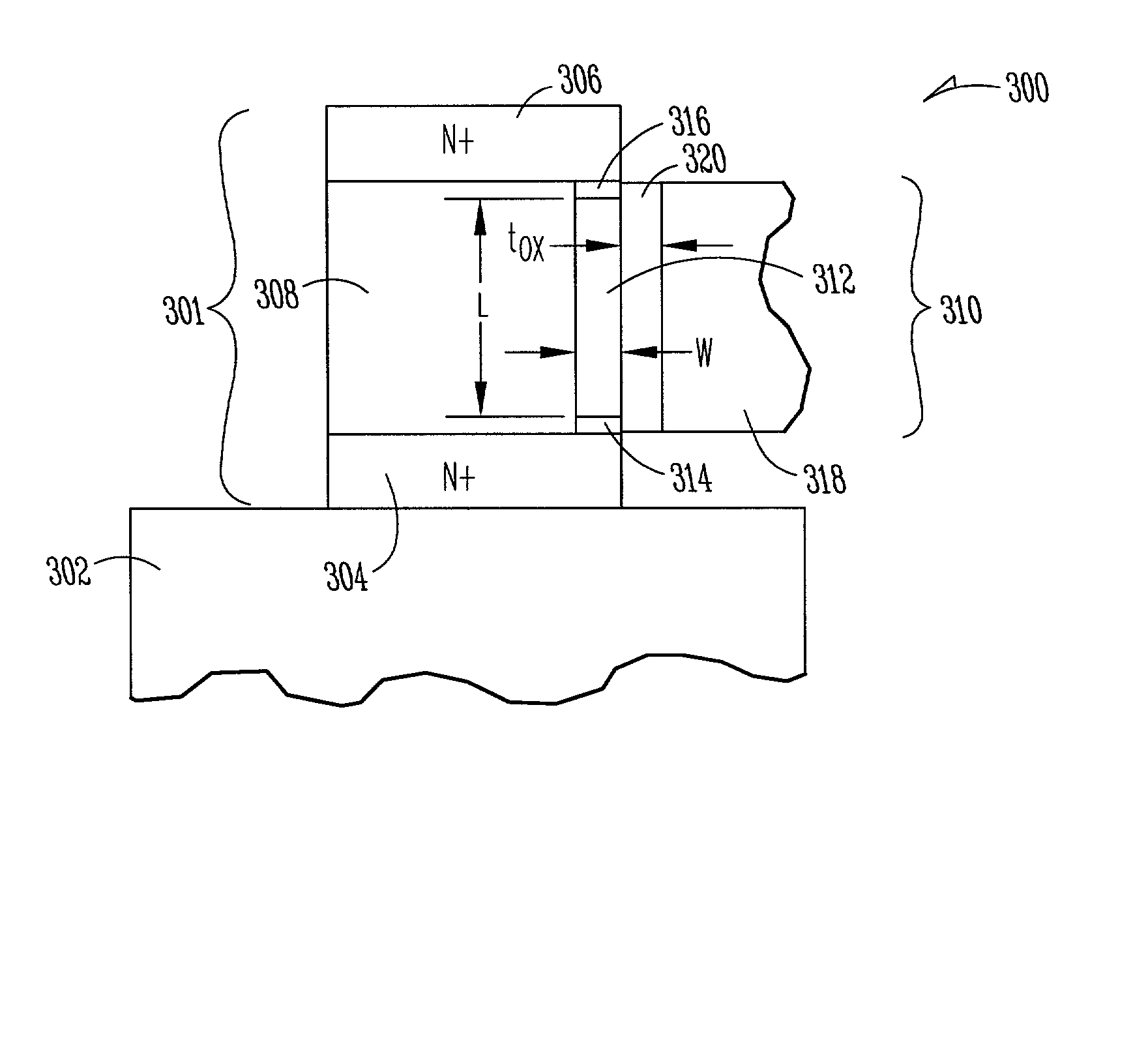
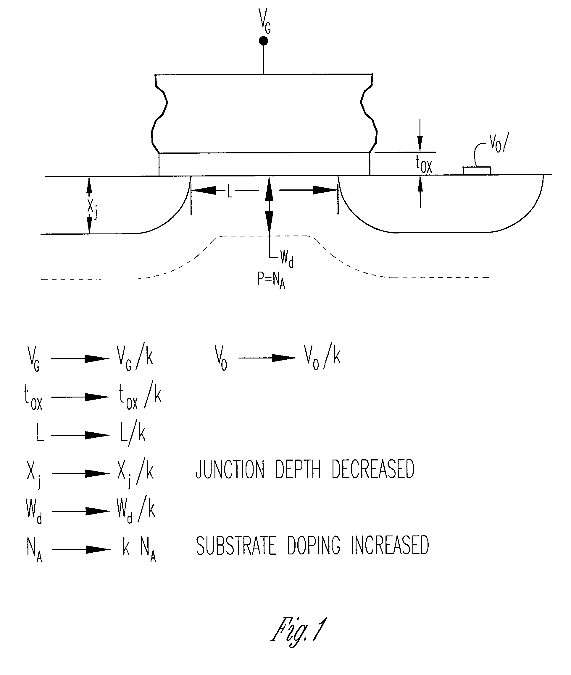
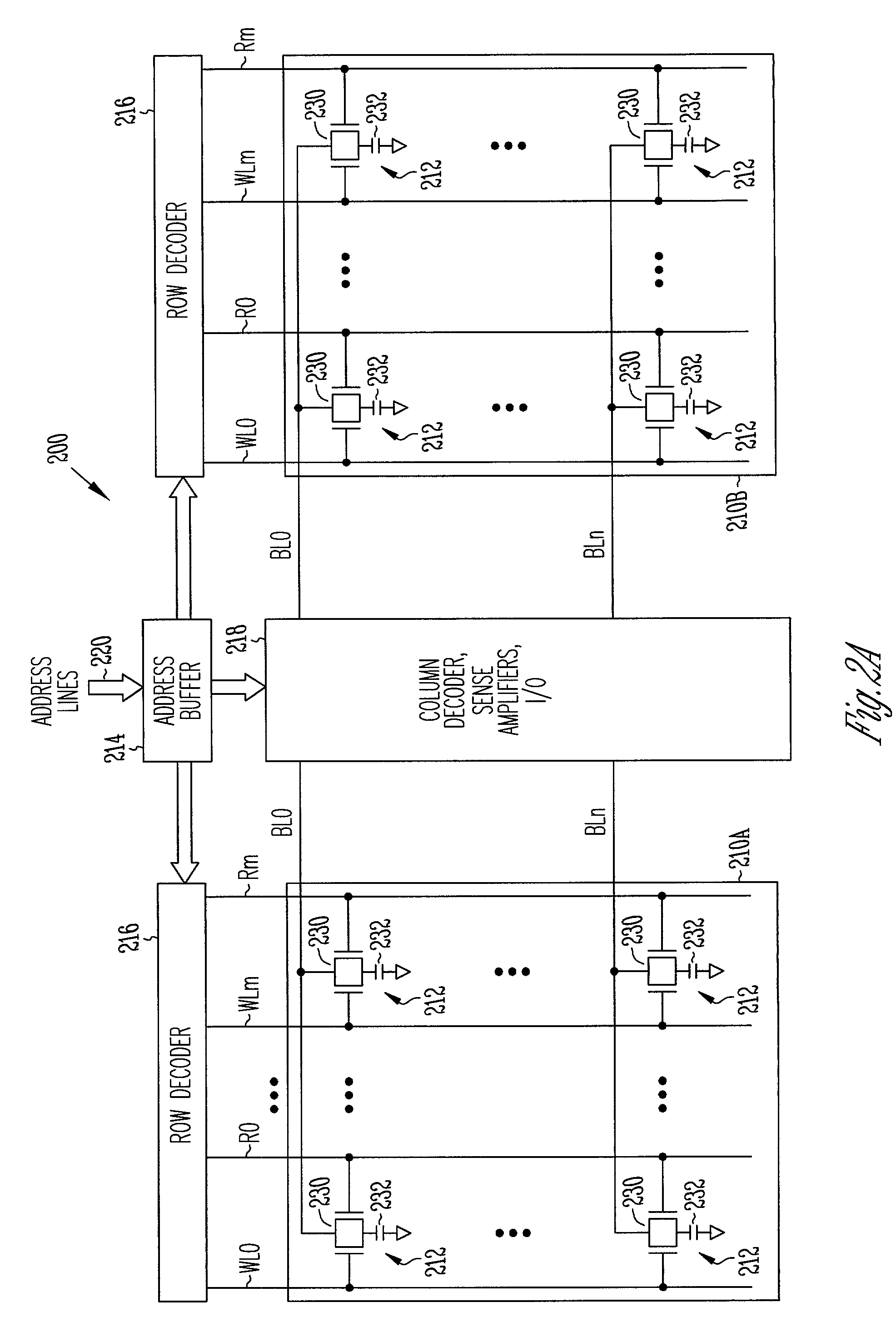
[0027] In the following detailed description of the invention, reference is made to the accompanying drawings which form a part hereof, and in which is shown, by way of illustration, specific embodiments in which the invention may be practiced. The embodiments are intended to describe aspects of the invention in sufficient detail to enable those skilled in the art to practice the invention. Other embodiments may be utilized and changes may be made without departing from the scope of the present invention. In the following description, the terms wafer and substrate are interchangeably used to refer generally to any structure on which integrated circuits are formed, and also to such structures during various stages of integrated circuit fabrication. Both terms include doped and undoped semiconductors, epitaxial layers of a semiconductor on a supporting semiconductor or insulating material, combinations of such layers, as well as other such structures that are known in the art. The fol...


PUM


Abstract

Structures and method for an open bit line DRAM device are provided. The open bit line DRAM device includes an array of memory cells. Each memory cell in the array of memory cells includes a pillar extending outwardly from a semiconductor substrate. The pillar includes a single crystalline first contact layer and a single crystalline second contact layer separated by an oxide layer. In each memory cell a single crystalline vertical transistor is formed along side of the pillar. The single crystalline vertical transistor includes an ultra thin single crystalline vertical first source/drain region coupled to the first contact layer, an ultra thin single crystalline vertical second source/drain region coupled to the second contact layer, an ultra thin single crystalline vertical body region which opposes the oxide layer and couples the first and the second source/drain regions, and a gate opposing the vertical body region and separated therefrom by a gate oxide. A plurality of buried bit lines are formed of single crystalline semiconductor material and disposed below the pillars in the array memory cells for interconnecting with the first contact layer of column adjacent pillars in the array of memory cells. Also, a plurality of word lines are included. Each word line is disposed orthogonally to the plurality of buried bit lines in a trench between rows of the pillars for addressing gates of the single crystalline vertical transistors that are adjacent to the trench.

Description

CROSS-REFERENCE TO RELATED APPLICATIONS[0001] This application is related to the following co-pending, commonly assigned U.S. patent applications: "Folded Bit Line DRAM with Ultra Thin Body Transistors," attorney docket no. 1303.004US1, Ser. No. ______, "Programmable Logic Arrays with Ultra Thin Body Transistors," attorney docket no. 1303.007US1, Ser. No. ______, "Memory Address and Decode Circuits with Ultra Thin Body Transistors," attorney docket no. 1303.006US1, Ser. No. ______,"Programmable Memory Address and Decode Circuits with Ultra Thin Body Transistors," attorney docket no. 1303.008US1, Ser. No. ______, "In Service Programmable Logic Arrays with Ultra Thin Body Transistors," attorney docket no. 1303.009US1, Ser. No. ______, and "Flash Memory with Ultra Thin Vertical Body Transistors," attorney docket no. 1303.003US1, Ser. No. ______, which are filed on even date herewith and each of which disclosure is herein incorporated by reference.FIELD OF THE INVENTION[0002] The presen...

Claims


Application Information

Patent Timeline
IPC IPC(8): H01L21/336H01L21/8242H01L27/088H01L27/108H01L29/78H01L21/8234H01L29/786
CPCH01L27/10814H01L27/10823H01L27/10876H01L27/10885H01L29/78642H01L29/0653H01L29/66666H01L29/7827H01L27/1203H10B12/315H10B12/34H10B12/053H10B12/482H10B12/00
Inventor FORBES, LEONARDAHN, KIE Y.
Owner MICRON TECH INC
Why Eureka
Try Eureka