Nonvolatile memory, semiconductor device and method of manufacturing the same

a semiconductor device and non-volatile memory technology, applied in semiconductor devices, semiconductor/solid-state device details, electrical devices, etc., can solve the problems of low writing/reading speed, dozens of times higher writing/reading speed than the magnetic disk, and difficulty in reducing siz

Inactive Publication Date: 2002-08-22
SEMICON ENERGY LAB CO LTD
View PDF71 Cites 47 Cited by
  • Summary
  • Abstract
  • Description
  • Claims
  • Application Information

AI Technical Summary

Benefits of technology

[0012] According to the present invention, a nonvolatile memory can be integrally formed with an arbitrary circuit constituted by using TFTs on an insulating substrate. Particularly, a memory cell, its driver circuit (typically, an address decoder) and other peripheral circuits are integrally formed on an insulating, substrate, thereby making it possible to provide a nonvolatile memory which can be reduced in size. Furthermore, an arbitrary circuit including TFTs that constitutes another semiconductor device is integrally formed on an insulating substrate, thereby making it possible to provide a semiconductor device including a nonvolatile memory, which can be reduced in size.
[0015] The semiconductor active layer of the memory TFT is formed thinner than that of the switching active layer, or is formed to have a thickness in the range of 1 to 100 nm (preferably 1 to 50 nm, more preferably 10 to 40 nm). The semiconductor active layer of the memory TFT is formed thin in this way, thereby allowing efficient writing as compared with the semiconductor active layer having a thicker thickness. This also signifies that writing can be performed at a lower driving voltage. At the same time, the memory cell has such a structure that can support an increased number of writings.
[0017] In the thus formed crystalline semiconductor layer, a memory TFT including the region having the first thickness as a semiconductor active layer and a switching TFT including the region having the second thickness as a semiconductor active layer are formed, thereby making it possible to manufacture a nonvolatile memory having a memory cell in which the semiconductor active layers of the memory TFT and the switching TFT are continuously formed. Furthermore, the semiconductor active layers are formed so that the first thickness is thinner than the second thickness, or the first thickness is 1 to 100 nm (preferably, 1 to 50 nm, more preferably, 10 to 40 nm), thereby allowing the manufacture of a nonvolatile memory according to the present invention.

Problems solved by technology

However, the magnetic disk has drawbacks such as a difficulty in reduction of size and low writing / reading speed.
On the other hand, although the semiconductor nonvolatile memory is inferior to the magnetic disk in terms of the memory capacity, its writing / reading speed is dozens of times higher than that of the magnetic disk.

Method used


Image

  • Nonvolatile memory, semiconductor device and method of manufacturing the same
  • Nonvolatile memory, semiconductor device and method of manufacturing the same
  • Nonvolatile memory, semiconductor device and method of manufacturing the same

Examples


embodiment 1

[Embodiment 1]

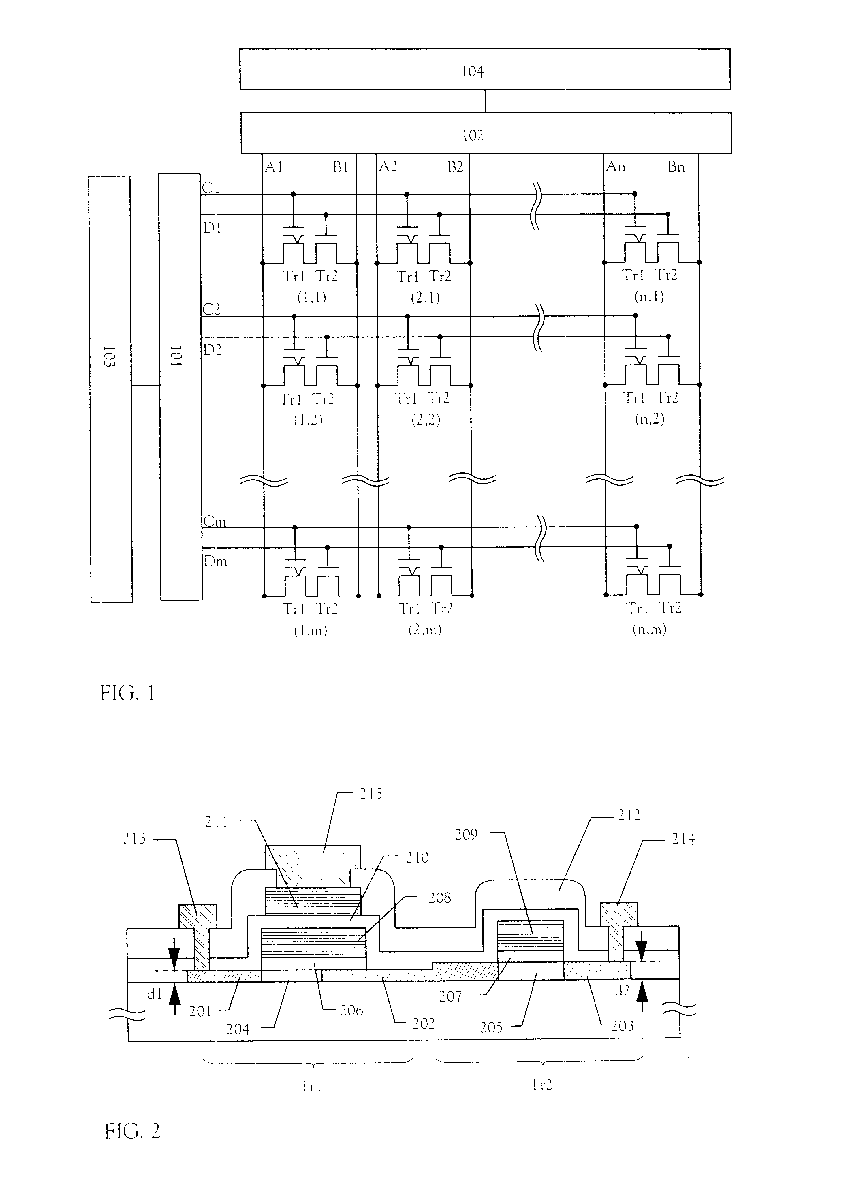
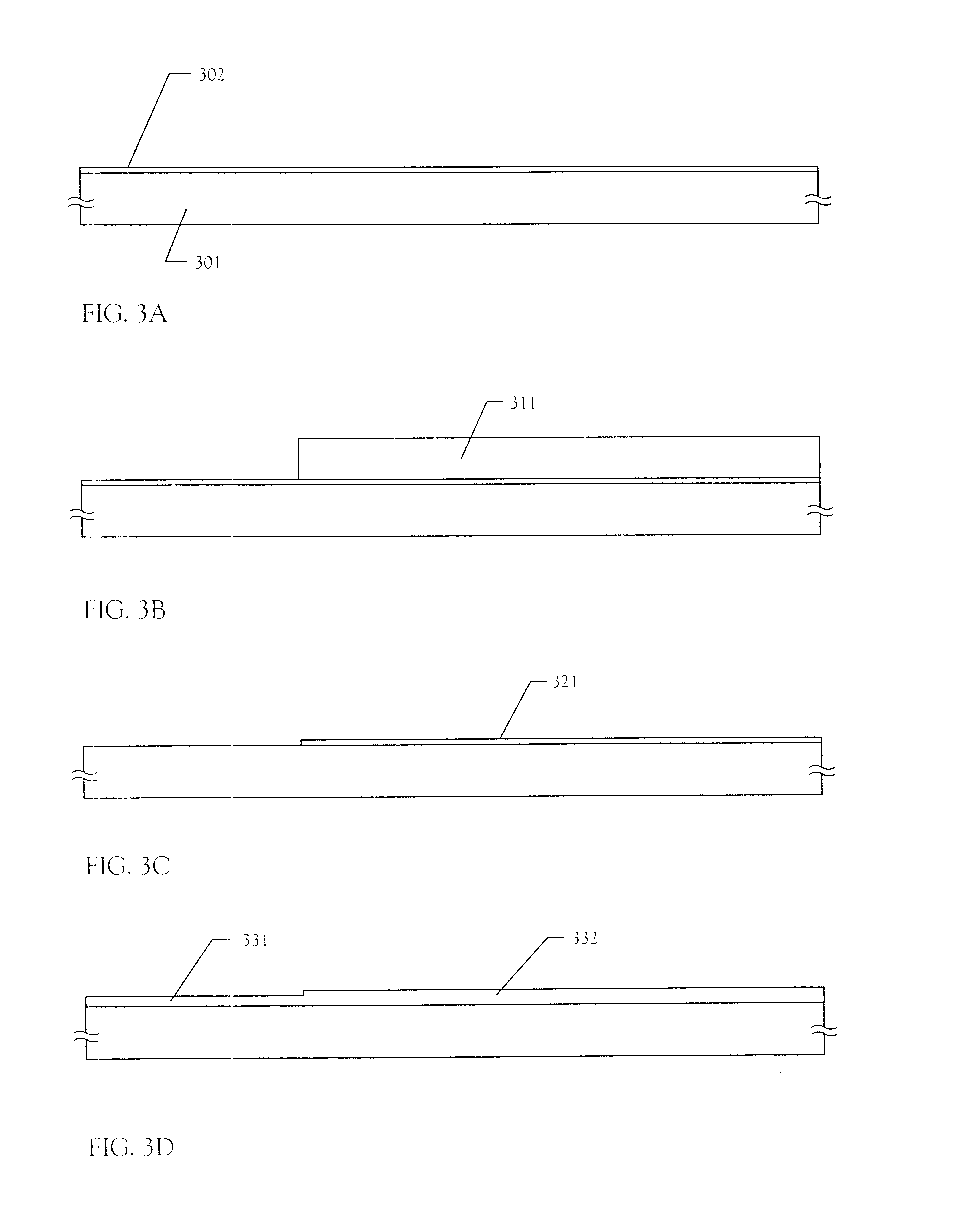
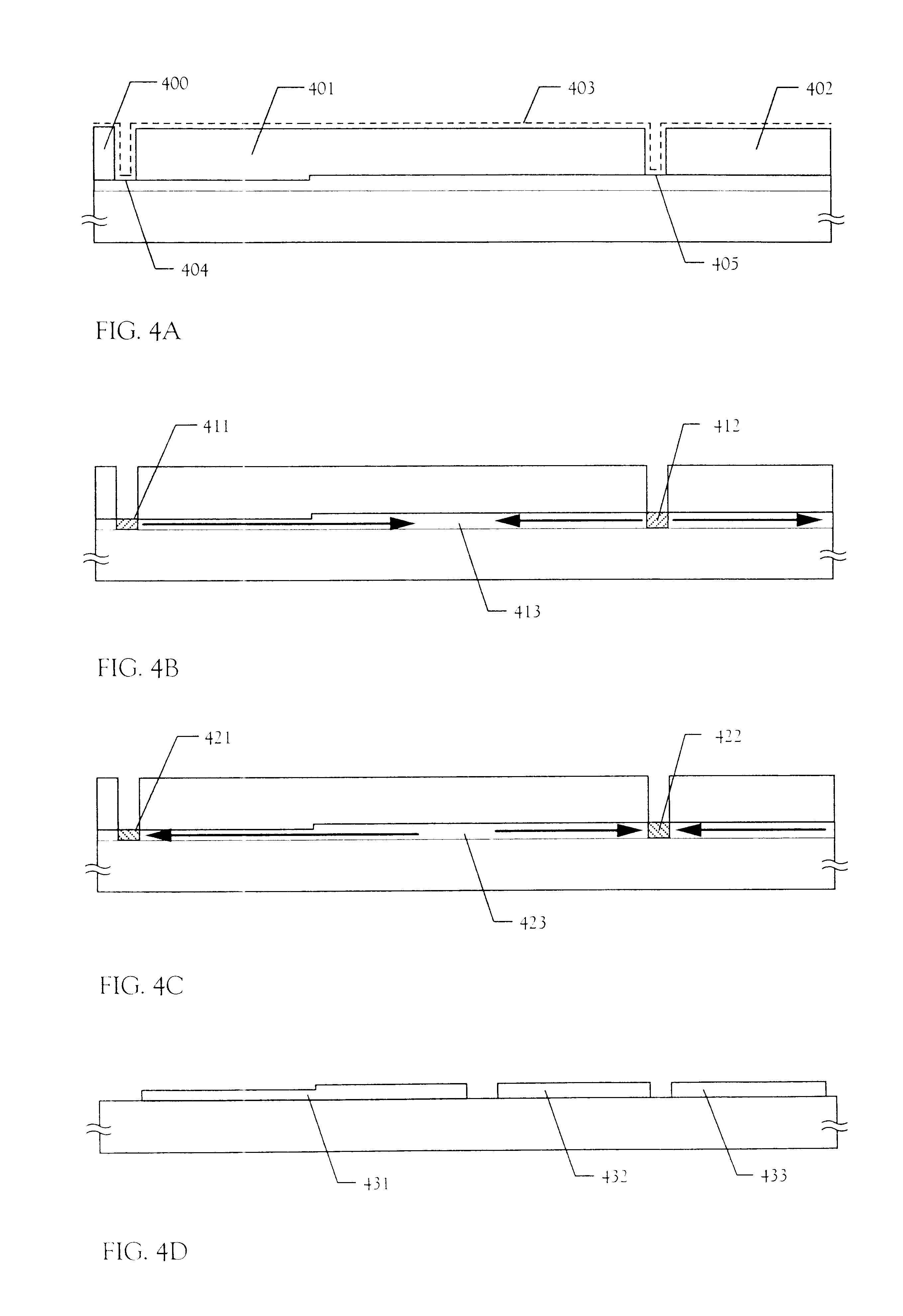
[0111] In Embodiment 1, a method of manufacturing a nonvolatile memory using the present invention will be described with reference to FIGS. 3A to 6D. In FIGS. 3A to 6D, a memory TFT (a p-channel TFT) and a switching TFT (a p-channel TFT) constituting a memory cell, and two TFTs (a p-channel TFT and an n-channel TFT) constituting a CMOS circuit that is representative as a circuit constituting an address decoder or other peripheral circuits are described as examples.

[0112] According to the manufacturing method of a nonvolatile memory described below, it is understood that the nonvolatile memory of the present invention can be integrally formed with any components of the semiconductor device that can be manufactured by using a thin film technique.

[0113] In order to realize a nonvolatile memory and a semiconductor device, which have memory cells, an address decoder and other circuits constituted by TFTs on the same insulating substrate, TFTs having enhanced properties in ...

embodiment 2

[Embodiment 2]

[0155] In this embodiment, the case where a nonvolatile memory is constituted with an inverted stagger TFT will be described with reference to FIGS. 9A through FIG. 11B. In FIGS. 9A through FIG. 11B, a memory TFT (a p-channel TFT) and a switching TFT (a p-channel TFT) constituting a memory cell, and two TFTs (a p-channel TFT and a n-channel TFT) constituting a CMOS circuit that is representative as a circuit constituting an address decoder or other peripheral circuits are taken as examples of TFTs constituting a nonvolatile memory according to the present invention.

[0156] Referring to FIG. 9A, a base film 902 made of a silicon oxide film is first formed on a glass substrate 901. Then, gate electrodes 903 through 906 are formed thereon. The gate electrode 903 serves as a control gate electrode of the memory TFT in the later step, while the gate electrode 904 serves as a gate electrode of the switching TFT in the later step. Although a chromium film having a thickness of...

embodiment 3

[Embodiment 3]

[0176] In the cross-sectional view of the memory cell shown in FIG. 2, the semiconductor active layer (thickness: d1) of the memory TFT is thinner than that (thickness: d2) of the switching TFT. However, it is sufficient to form these semiconductor active layers so that d1 is 1 to 100 nm (preferably, 1 to 50 nm, more preferably, 10 to 40 nm) and d2 is 1 to 150 nm (preferably, 10 to 100 nm). Particularly, the semiconductor active layer of the memory TFT and the semiconductor active layer of the switching TFT may have the same thickness.

[0177] The semiconductor active layers of TFTs constituting a driver circuit of the memory cells and other peripheral circuits may be formed so as to have the same thickness as that of the semiconductor active layer of the memory TFT or to have a greater thickness than that of semiconductor active layer of the memory TFT as long as a driving frequency of the circuit is not lowered.

[0178] For this embodiment, the manufacture methods of Emb...


PUM


Abstract

The present invention provides a nonvolatile memory that can be integrally formed with other semiconductor devices and can be reduced in size. A memory TFT, a switching TFT and other peripheral circuits constituting a nonvolatile memory are integrally formed on a substrate by TFTs. The memory TFT and the switching TFT are formed on the same semiconductor active layer, and a semiconductor active layer of the memory TFT is formed thinner than semiconductor active layers of the other TFTs. As a result, a nonvolatile memory that is hardly deteriorated and that can be reduced in size is provided, in which writing / erasing for the memory TFT can be realized at a low voltage.

Description

[0001] 1. Field of the invention[0002] The present invention relates to a nonvolatile memory including thin-film transistors (hereinafter, abbreviated as TFTs) formed by using an SOI (Silicon On Insulator) technique and a method of manufacturing the same. Particularly, the present invention relates to a nonvolatile memory integrally formed with peripheral circuits such as a driver circuit on a substrate having an insulating surface, particularly, to an EEPROM (Electrically Erasable and Programmable Read Only Memory). Moreover, the present invention also relates to a semiconductor device including a nonvolatile memory integrally formed with an arbitrary circuit including TFTs on a substrate having an insulating surface.[0003] In the specification, the term semiconductor device generically indicates the devices that function by taking advantage of semiconductor properties; for example, electro-optical devices as represented by a liquid crystal display device and an EL display device, ...

Claims


Application Information

Patent Timeline
Patent Type & Authority Applications(United States)
IPC IPC(8): H01L21/77H01L21/8247H01L21/84H01L27/115H01L27/12H01L29/786
CPCH01L27/115H01L27/11521H01L27/1214H01L29/78672H01L27/1233H10B69/00H10B41/30
Inventor KOYAMA, JUNKATO, KIYOSHI
Owner SEMICON ENERGY LAB CO LTD
Why Eureka
Try Eureka