Method and apparatus for registration control in production by imaging

Inactive Publication Date: 2002-08-29
KODAK IL
View PDF0 Cites 27 Cited by
  • Summary
  • Abstract
  • Description
  • Claims
  • Application Information

AI Technical Summary

Benefits of technology

0007] According to one aspect of the present invention, there is provided a method of imaging an overlying pattern over an underlying pattern on a substrate, each pattern being defined by image data to be applied at nominal (i.e., theoretical or desired) locations according to scanning control data, the method comprising: determining deviations between the actual l

Problems solved by technology

The interlayer registration of the conductive patterns is of critical importance and becomes increasingly problematical as the dimensions of the conductive patterns decrease in size, and as the panels increase in size to improve productivity.
However, phototools of the plastic type tend to change in dimensions with changes in temperature and/or humidity, and phototools of

Method used


Image

  • Method and apparatus for registration control in production by imaging
  • Method and apparatus for registration control in production by imaging
  • Method and apparatus for registration control in production by imaging

Examples


Embodiment Construction

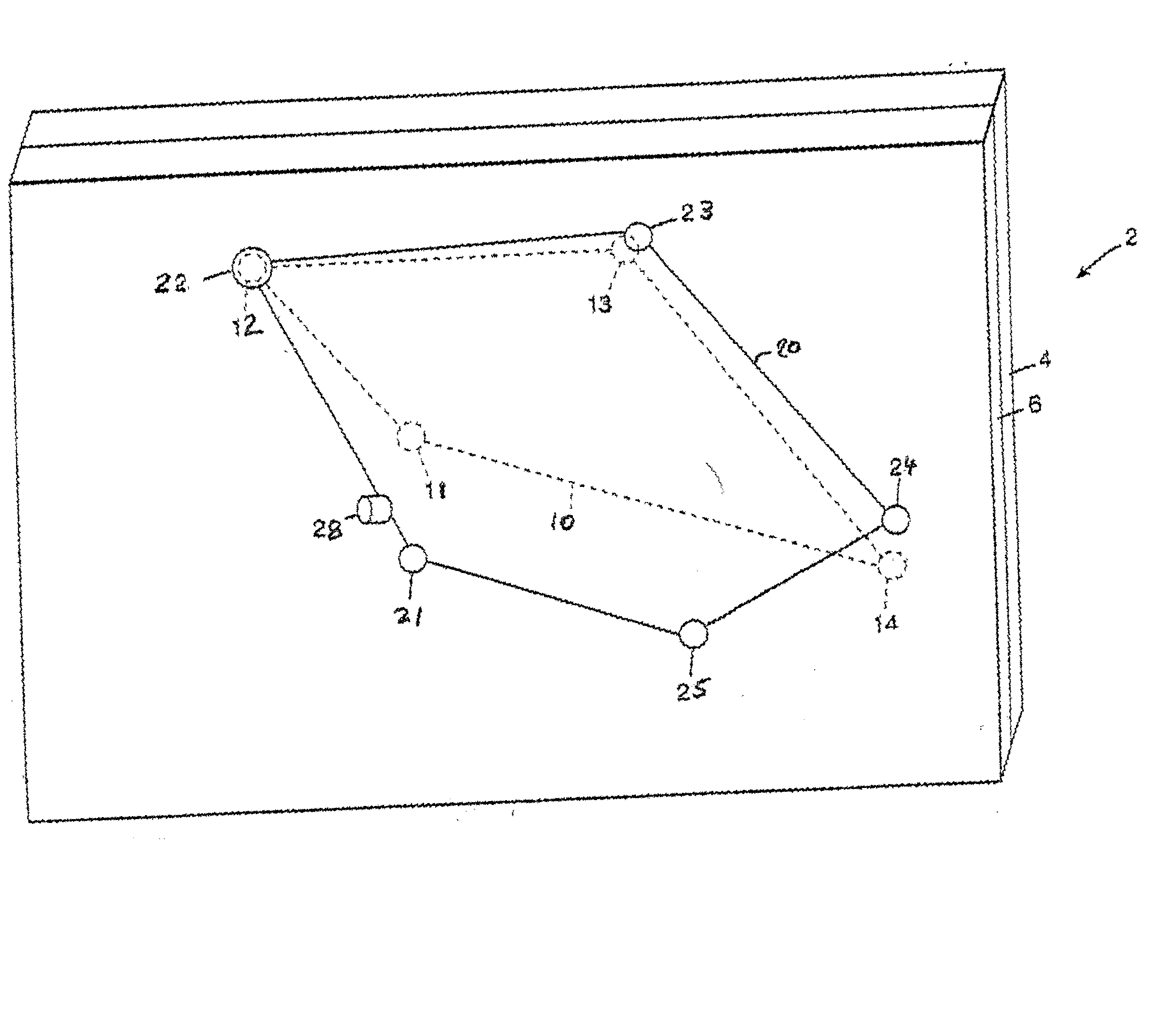
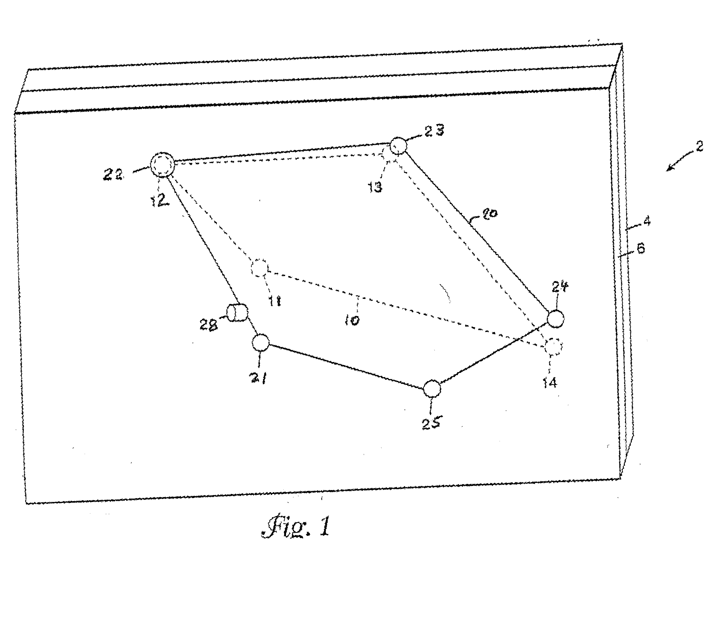
[0025] With reference first to FIG. 1, this figure shows only two layers of a multi-layer PCB 2, namely an underlying layer 4, and an overlying layer 6. The underlying layer 4 is formed with a conductive or non-conductive pattern, schematically shown by broken lines 10, including a plurality of connection sites 11, 12, 13, and 14, respectively. The overlying layer 6 to be formed thereover also includes a conductive pattern, schematically shown by full lines 20, having a plurality of connection sites 21, 22, 23, 24 and 25, respectively.

[0026] As seen in FIG. 1, connection site 12 of the underlying conductive pattern 10 is in perfect registration with connection site 22 in the overlying pattern 20, so that a conductive pin, such as schematically shown at 28, may be passed through a hole formed through the connection sites 12, 22, to make an electrical connection between the two conductive patterns 10, 20 at these connection sites. While FIG. 1 illustrates the connection to the two con...


PUM


Abstract

A method and apparatus for imaging an overlying conductive pattern over an underlying conductive pattern on a substrate, by determining deviations between the actual locations and the nominal locations of predetermined reference targets in the underlying conductive pattern on the substrate; and utilizing the determined deviations for modifying the scanning control data used for imaging the image data of the overlying conductive pattern in order to reduce misregistration thereof with respect to the underlying conductive pattern. Preferably, the reference targets are predetermined connection sites in the underlying conductive pattern to be precisely located with respect to connection sites in the overlying conductive pattern. The reference features may be assigned different weights according to their registration importance, and the deviations may be determined according to a threshold which varies with the weight assigned to the respective reference feature.

Description

FIELD AND BACKGROUND OF THE INVENTION[0001] The present invention relates to registration control in various production methods that use imaging. This includes, but is not limited to, Electronics Components (ELC), Flat Panel Displays (FPD), various conductive and non-conductive patterns or holes on / in PCBs, masks for soldering, plating, etching or plasma etching, or hole plug curring. The invention is particularly useful in producing multi-layer PCBs in accordance with the laser direct imaging (LDI) process, and is therefore described below particularly with respect to this process.[0002] Multi-layer PCBs (sometimes referred to as PWBs or printed wiring boards) are widely used in electronic systems. Such PCBs may include as many as 20 or 30 layers, each having its own electrically conductive pattern, with various layers electrically connected together by interlayer connections, such as pins, posts, plated-through-holes (PTHs), pads and the like. The interlayer registration of the co...

Claims


Application Information

Patent Timeline
IPC IPC(8): G03F7/20G03F9/00G06T1/00H05K1/02H05K3/00H05K3/46
CPCG03F7/70383G03F9/00H05K1/0269H05K3/0008H05K3/0082H05K3/4644H05K3/4679H05K2201/09918
Inventor CABIRI, OZMIKLETZKI, EFFRAIMATIYA, YOSSEF
Owner KODAK IL
Why Eureka
Try Eureka