Method of and apparatus for correctly transmitting signals at high speed without waveform distortion

a signal transmission and waveform technology, applied in the field of signal transmission technique, can solve the problems of affecting the performance of drams (dynamic random access memories) and processors, and affecting the performance of computers

Inactive Publication Date: 2002-09-12
FUJITSU LTD
View PDF0 Cites 56 Cited by
  • Summary
  • Abstract
  • Description
  • Claims
  • Application Information

AI Technical Summary

Benefits of technology

0037] The reception signal determination circuit may include a reception timing detector for receiving a sequence of reference codes alternating between 0 and 1, detecting the reference codes, and determining reception timing used as a threshold to detect 0s and is in a receive...

Problems solved by technology

In particular, an improvement in the performance of DRAMs (dynamic random access memories) and processors is d...

Method used


Image

  • Method of and apparatus for correctly transmitting signals at high speed without waveform distortion
  • Method of and apparatus for correctly transmitting signals at high speed without waveform distortion
  • Method of and apparatus for correctly transmitting signals at high speed without waveform distortion

Examples


first embodiment

[0134] FIG. 4 shows a driver circuit for transmitting signals according to the first aspect of the present invention, FIG. 5 shows a variable gain unit of the driver circuit, and FIG. 6 shows an amplifier of the driver circuit.

[0135] The driver circuit has a front driver 4 that consists of an amplifier 41, a variable gain unit 42, and a feedback resistor 43. The driver circuit also has an output driver 1 that consists of an n-channel MOS transistor (NMOS transistor) 11 and a p-channel MOS transistor (PMOS transistor) 12.

[0136] To drive a load resistor of, for example, several tens of ohms, the output driver 1 is a source follower employing the large NMOS transistor 11 and PMOS transistor 12 to realize a gain of about 1.

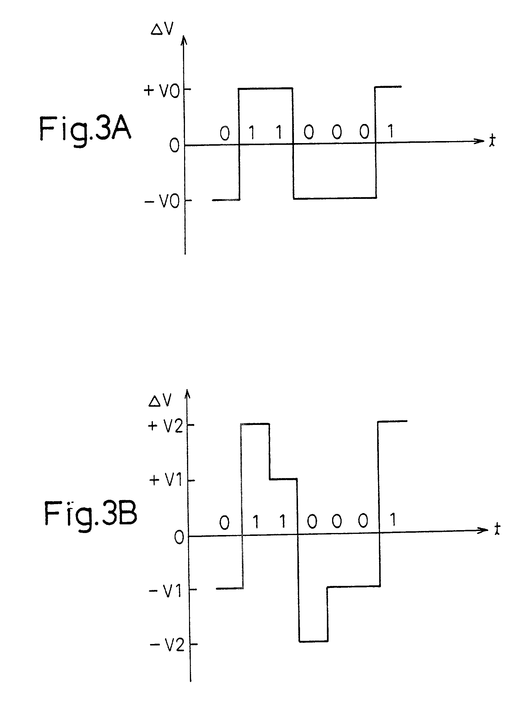
[0137] In FIG. 5, the variable gain unit 42 consists of transfer gates 421 to 42n that are switched in response to control signals (control codes) .phi.1 to .phi.n provided by a level adjuster serving as a control signal generator. When one (for example, .phi.1) of th...

second embodiment

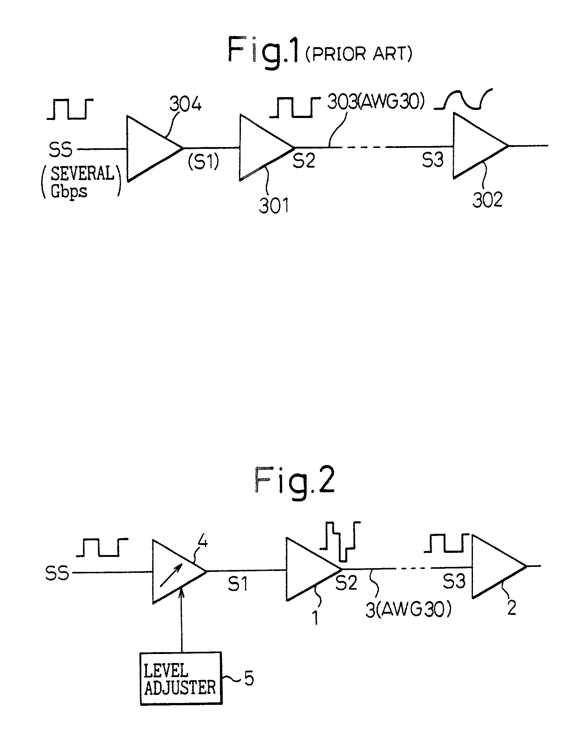
[0140] FIG. 7 shows a driver circuit for transmitting signals according to the first aspect of the present invention.

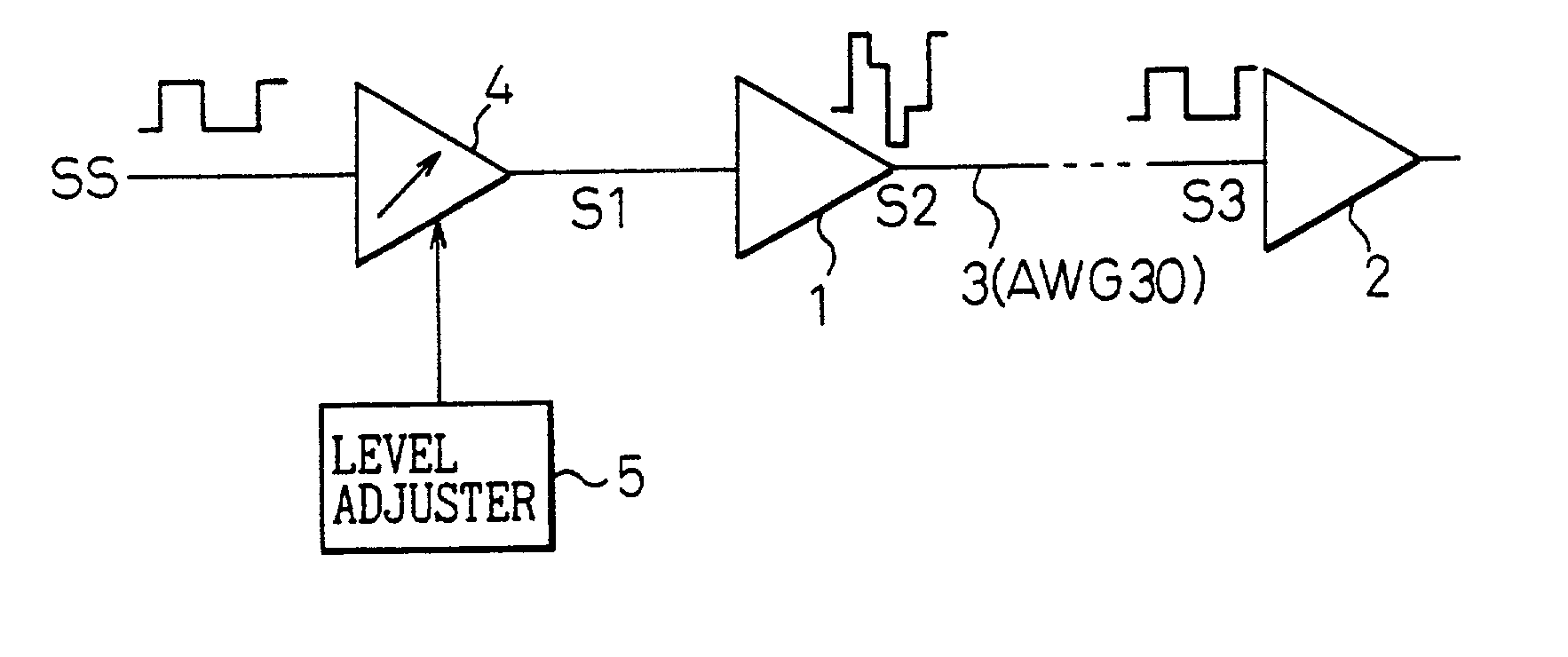
[0141] As is apparent from comparison between FIGS. 7 and 4, a front driver 4 with a level adjuster (control signal generator) 5 of FIG. 7 is the same as that of FIG. 4, and an output driver 1 of FIG. 7 differs from that of FIG. 4.

[0142] The output driver 1 of FIG. 7 has a feedback amplifier 11. The resistance of a feedback resistor 13 is two to four times as large as that of a resistor 12 connected to an inverting input terminal of the amplifier 11, thereby providing a gain of two to four times as large as a usual value. For example, the resistor 12 has a resistance of 1 K.OMEGA. and the feedback resistor 13 has a resistance of 3 K.OMEGA. so that the amplifier 11 may provide a gain of about 3.

[0143] The output driver 1 amplifies a variable output signal S1 from the front driver 4 and provides an amplified output signal S2. Since the loop gain of the output driver 1 i...

third embodiment

[0144] FIG. 8 shows a front driver of a driver circuit for transmitting signals according to the first aspect of the present invention, and FIG. 9 shows an output driver of the driver circuit.

[0145] In FIG. 8, the front driver 4 is formed as a current limiting inverter consisting of PMOS transistors 44 and 45 and NMOS transistors 46 and 47 that are connected in series. A signal SS is commonly supplied to the gates of the PMOS transistor 44 and NMOS transistor 47. The gate of the PMOS transistor 45 receives a control voltage Vcp, and the gate of the NMOS transistor 46 receives a control voltage Vcn.

[0146] In FIG. 9, the output driver 1 is formed as a constant current circuit employing current mirror circuits. An output terminal of the output driver 1 for providing an output signal S2 is connected to a load register 10 to form a current / voltage converter for converting an input current S1 from the front driver 4 into an output voltage S2.

[0147] The output driver 1 consists of PMOS tra...


PUM


Abstract

A driver circuit transmits a signal to a receiver circuit through a signal transmission line. The driver circuit has an output driver, a front driver, and a level adjuster. The front driver drives the output driver, and the level adjuster adjusts the output level of the front driver. The output driver generates a signal whose level is variable in response to an output level of the front driver.

Description

BACKGROUND OF THE INVENTION[0001] 1. Field of the Invention[0002] The present invention relates to a signal transmission technique. More particularly, a first aspect of the present invention relates to a driver circuit used for transmitting signals between LSI chips or between elements or circuit blocks in an LSI chip, and a second aspect of the present invention relates to a receiver circuit and signal transmission system capable of transmitting signals at high speed. Further, a third aspect of the present invention relates to a timing signal generator circuit of a wide range of operation frequencies, and a fourth aspect of the present invention relates to a signal transmission technique involving the driver circuit, receiver circuit, and signal transmission system, capable of transmitting signals at high speed.[0003] 2. Description of the Related Art Recently, the performance of information processing equipment such as computers has improved greatly. In particular, an improvement ...

Claims


Application Information

Patent Timeline
IPC IPC(8): H04B1/10G11C7/10G11C7/22G11C11/4076G11C11/4096H03K19/0185H03L7/07H03L7/081H04L25/02H04L25/03H04L25/10
CPCG11C7/1012G11C7/1048G11C7/1051G11C7/1069G11C7/22G11C7/222G11C8/08G11C11/4076G11C11/4096H03K19/018571H03L7/07H03L7/0812H04L25/0272H04L25/0274H04L25/0276H04L25/0278H04L25/028H04L25/0282H04L25/0288H04L25/0292H04L25/03878H04L25/03885H04L25/10H03L7/0816E04F13/0733E04F13/088
Inventor TAMURA, HIROTAKATAKAUCHI, HIDEKICHEUNG, TSZ-SHINGGOTOH, KOHTAROH
Owner FUJITSU LTD
Why Eureka
Try Eureka