

Method of preparing copper metallization die for wirebonding
a technology of wirebonding and copper metallization die, which is applied in the direction of semiconductor devices, semiconductor/solid-state device details, electrical equipment, etc., can solve the problems of electrical short circuits, corrosion, and relatively quick oxidation of copper, and achieve less oxidation and oxidation. , the effect of reducing the oxidation of copper pads
- Summary
- Abstract
- Description
- Claims
- Application Information
AI Technical Summary
Problems solved by technology
Method used
Image

Examples
Embodiment Construction
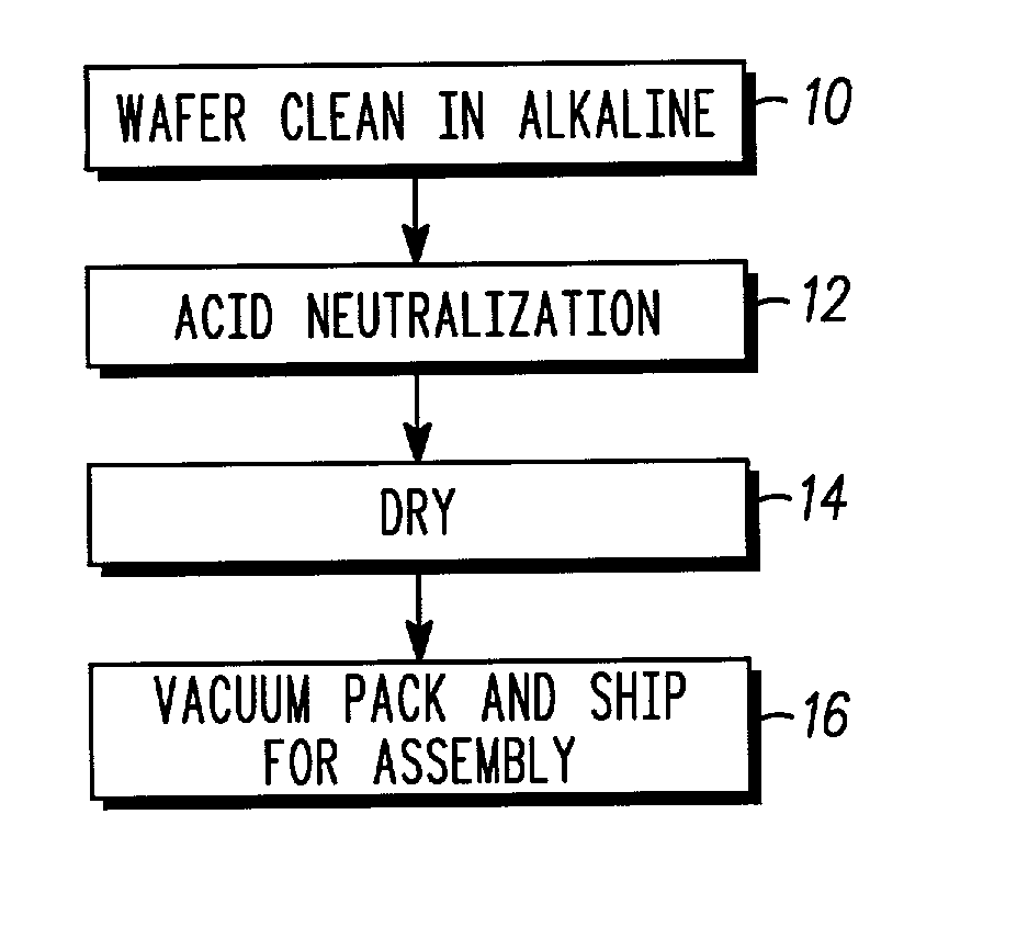
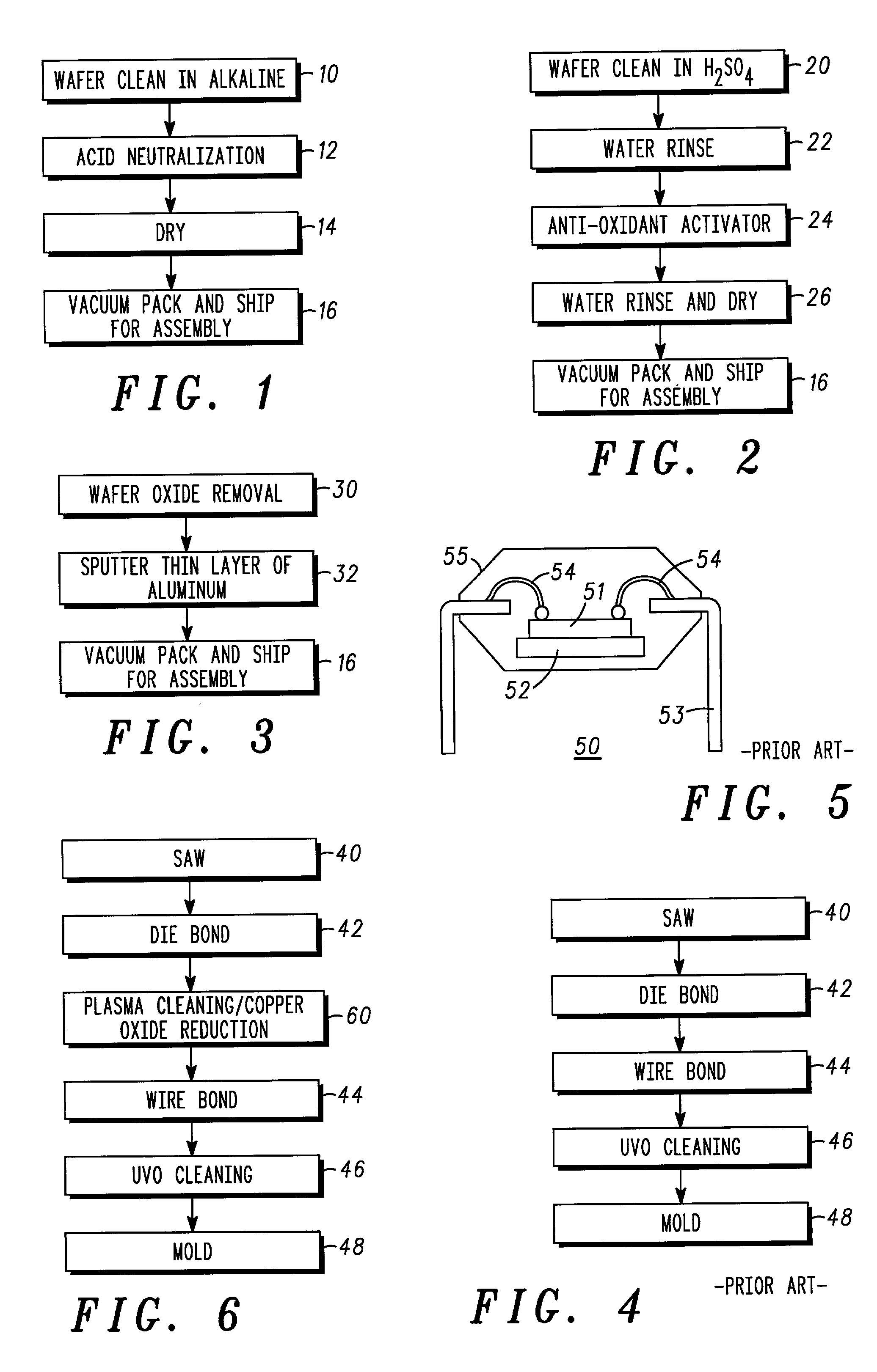
[0021] The detailed description set forth below in connection with the appended drawings is intended as a description of the presently preferred embodiments of the invention, and is not intended to represent the only forms in which the present invention may be practiced. The description sets forth sequences of steps for performing the procedures in connection with the illustrated embodiments. It is to be understood, however, that the same or equivalent functions and sequences may be accomplished by different embodiments that are intended to be encompassed within the spirit and scope of the invention. In the drawings, like numerals are used to indicate like elements throughout.
[0022] As previously discussed, it has become popular to fabricate integrated circuits using copper interconnect metallization technology due to the advantages in electrical performance and cost. In order to prevent intermetallic phases, the ICs are provided with copper pads. Typically, wire bonding of the IC w...
PUM
| Property | Measurement | Unit |
|---|---|---|
| thick | aaaaa | aaaaa |
| thickness | aaaaa | aaaaa |
| pressure | aaaaa | aaaaa |
Abstract
Description
Claims
Application Information