Method of manufacturing semiconductor integrated circuit device and semiconductor manufacturing apparatus

a manufacturing apparatus and integrated circuit technology, applied in semiconductor/solid-state device testing/measurement, instruments, transportation and packaging, etc., can solve the problems of optical sensors not being able to detect the breakage or crack in a part of the wafer completely, the manufacturing cost of the semiconductor integrated circuit device is problematically increased, and the number of defective wafers produced is increased

Inactive Publication Date: 2002-09-12
RENESAS TECH CORP
View PDF3 Cites 14 Cited by
  • Summary
  • Abstract
  • Description
  • Claims
  • Application Information

AI Technical Summary

Benefits of technology

0013] When transporting the wafer with the breakage and the crack to the next chamber and performing, for example, a deposition step of a metal film by the PVD method, the metal film is deposited on an electrostatic chuck to fix the wafer, and as a result, the electrostatic chuck and other shield parts in the chamber have to be replaced disadvantageously. Therefore, maintenance including cleaning is needed to all of the chambers through which the wafer with the breakage and the crack passes. Consequently, it disadvantageously takes much time to restart to manufacture the semiconductor integrated circuit device. In addition, since the parts replacement and the cleaning are required, the manufacturing cost of the semiconductor integrated circuit device is problematically increased.
0014] Also, if fragments of the broken wafer are scattered to other wafers stored in the load-lock chamber, the stored wafers are also damaged and become defective. Recently, transition to larger diameter wafers has been accelerated, but the larger diameter causes the increase of cost per wafer. If the number of defective wafers produced is increased, the manufacturing cost of the semiconductor integrated circuit device is further increased. Therefore, it is further necessary to take measures to the problem described above.

Problems solved by technology

That is, during the processes performed to a wafer in each chamber such as the film formation by the CVD (Chemical Vapor Deposition) method, the film formation by the PVD (Physical Vapor Deposition) method, and the dry etching, damages such as breakage and crack often occur in a part of the wafer due to thermal stress applied thereto during the process or an accident during the transportation thereof.
If a stress is applied to a wafer having the crack, the wafer may be broken from the crack.
Therefore, such an optical sensor can not detect the breakage or the crack in a part of the wafer completely.
When transporting the wafer with the breakage and the crack to the next chamber and performing, for example, a deposition step of a metal film by the PVD method, the metal film is deposited on an electrostatic chuck to fix the wafer, and as a result, the electrostatic chuck and other shield parts in the chamber have to be replaced disadvantageously.
Consequently, it disadvantageously takes much time to restart to manufacture the semiconductor integrated circuit device.
In addition, since the parts replacement and the cleaning are required, the manufacturing cost of the semiconductor integrated circuit device is problematically increased.
Also, if fragments of the broken wafer are scattered to other wafers stored in the load-lock chamber, the stored wafers are also damaged and become defective.
Recently, transition to larger diameter wafers has been accelerated, but the larger diameter causes the increase of cost per wafer.
If the number of defective wafers produced is increased, the manufacturing cost of the semiconductor integrated circuit device is further increased.

Method used


Image

  • Method of manufacturing semiconductor integrated circuit device and semiconductor manufacturing apparatus
  • Method of manufacturing semiconductor integrated circuit device and semiconductor manufacturing apparatus
  • Method of manufacturing semiconductor integrated circuit device and semiconductor manufacturing apparatus

Examples


first embodiment

[0071] (First Embodiment)

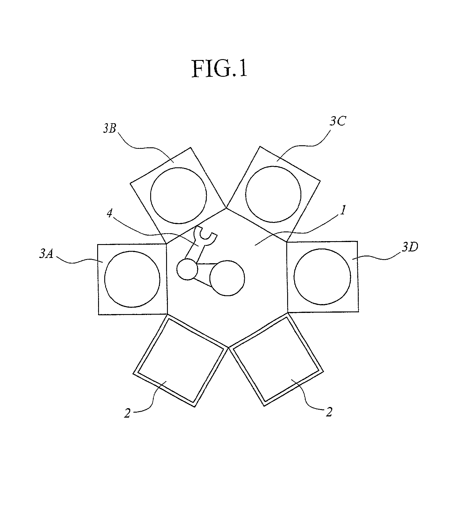
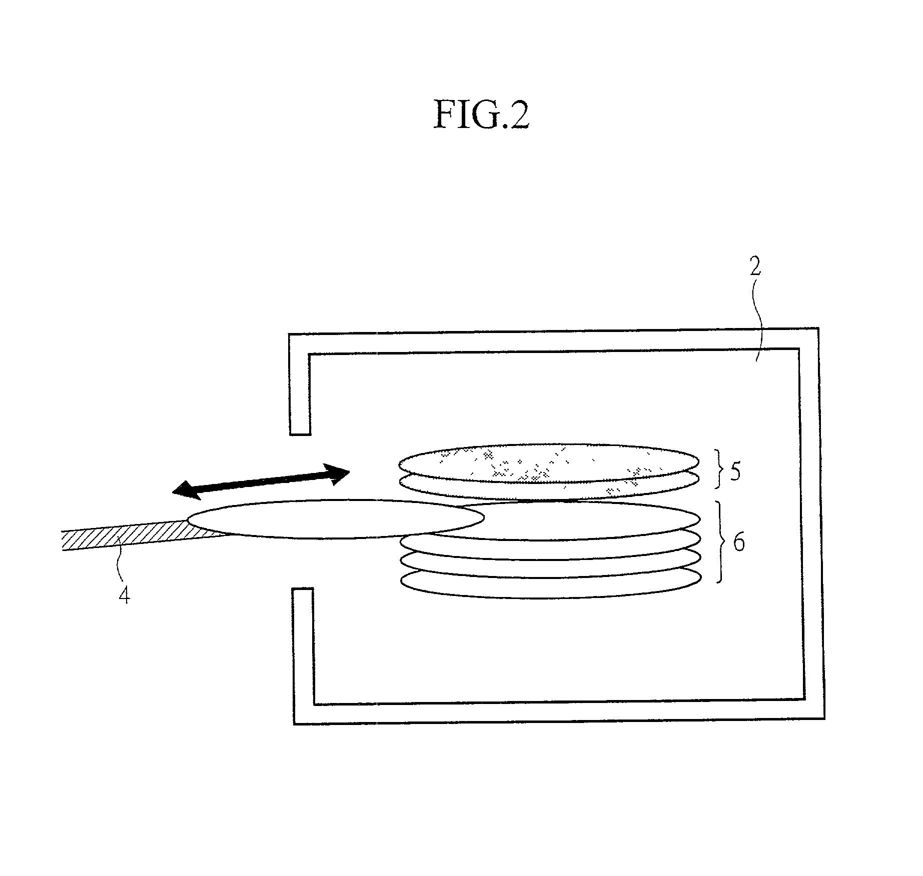
[0072] FIG. 1 shows a block diagram of a semiconductor manufacturing apparatus according to the first embodiment, in which a multi-chamber system is employed.

[0073] This semiconductor manufacturing apparatus is a single wafer processing type semiconductor manufacturing apparatus provided with a transport chamber 1, load-lock chambers 2, and process chambers 3A to 3D. A robot arm 4 is provided in the transport chamber 1, and the robot arm 4 can transport a wafer to the load-lock chambers 2 or to the process chambers 3A to 3D. In the process chambers 3A to 3D, various processes are performed to a wafer. The insides of the transport chamber 1, the load-lock chambers 2, and the process chambers 3A to 3D are kept in vacuum, and the transportation of a wafer can be performed without exposing the wafer to the outer atmosphere. In other words, in the semiconductor manufacturing apparatus in this first embodiment, various processes can be performed to a wafer without...

second embodiment

[0135] (Second Embodiment)

[0136] The method of manufacturing a semiconductor integrated circuit device according to the second embodiment is another example of the method of manufacturing a semiconductor integrated circuit device using the semiconductor manufacturing apparatus according to the first embodiment.

[0137] The method of manufacturing a semiconductor integrated circuit device according to the second embodiment will be described by the use of FIGS. 26 to 31.

[0138] The method of manufacturing a semiconductor integrated circuit device according to the second embodiment is identical to that in the first embodiment until the process proceeds to the step described by the use of FIGS. 14 to 19.

[0139] Thereafter, as shown in FIG. 26, a conductive film 40C made of, for example, TiN is deposited on the entire surface of a semiconductor substrate 1 by the sputtering method. Note that the deposition step of the conductive film 40C is carried out by using the semiconductor manufacturin...


PUM

PropertyMeasurementUnit
radiusaaaaaaaaaa
thicknessaaaaaaaaaa
temperatureaaaaaaaaaa

Abstract

Disclosed is a technique capable of suppressing the damage of a semiconductor manufacturing apparatus due to the breakage or the crack to the minimum by surely detecting the breakage or the crack on a part of a wafer in a semiconductor manufacturing apparatus of a multi-chamber system. An entire image of a wafer is photographed by a camera in each time when the wafer is processed, and the photographed image is processed by a discrimination unit, thereby determining the presence of the breakage or the crack on the wafer. When the breakage or the crack is detected, an error signal is transmitted from the discrimination unit to a computer that controls the semiconductor manufacturing apparatus, and the operations of the process chamber and the transport chamber used immediately before the detection of the breakage or the crack on the wafer are stopped.

Description

TECHNICAL FIELD OF THE INVENTION[0001] The present invention relates to a method of manufacturing a semiconductor integrated circuit device and to a semiconductor manufacturing apparatus, more particularly, to a technique effectively applicable to a method of manufacturing a semiconductor integrated circuit device, using a semiconductor manufacturing apparatus having a plurality of chambers.BACKGROUND OF THE INVENTION[0002] Recently, with higher integration and scaling down of a semiconductor device, the method of manufacturing a semiconductor integrated circuit device using a batch-type semiconductor manufacturing apparatus in which a great number of semiconductor wafers (hereinafter, referred to as wafer) are processed simultaneously has had difficulty adapting to such strict process conditions. Since the batch-type semiconductor manufacturing apparatus has a limitation in its ability to secure the accuracy and uniformity in processing a semiconductor device, a breakthrough in tec...

Claims


Application Information

Patent Timeline
Patent Type & Authority Applications(United States)
IPC IPC(8): G01N21/956C23C14/52C23C14/56C23C16/52C23C16/54G06T1/00H01L21/00H01L21/285H01L21/3205H01L21/66H01L21/677H01L21/768
CPCC23C14/52C23C14/568C23C16/52C23C16/54H01L21/2855H01L21/32051H01L21/67288H01L21/76804H01L22/20
Inventor KAWAKAMI, KAZUYASUZUKI, YUKIHIROOKUTANI, KENKAJITA, SUSUMUHASHIMOTO, TAKESHI
Owner RENESAS TECH CORP
Why Eureka
Try Eureka