Method of manufacturing a semiconductor device

a manufacturing method and semiconductor technology, applied in semiconductor devices, instruments, electrical devices, etc., can solve problems such as the variation of the taper angle of the resist pattern side wall

Inactive Publication Date: 2002-09-12
SEMICON ENERGY LAB CO LTD
View PDF0 Cites 19 Cited by
  • Summary
  • Abstract
  • Description
  • Claims
  • Application Information

AI Technical Summary

Benefits of technology

0012] It is an object of the present invention to provide an semiconductor device formed of inverted s

Problems solved by technology

Since various dimensions of circuit patterns exist in a liquid crystal display, deformation in the resist pattern with variation in taper angle depending on variation in the area of the resist pattern influences the etched shape, and thus is a critical problem.
In

Method used


Image

  • Method of manufacturing a semiconductor device
  • Method of manufacturing a semiconductor device
  • Method of manufacturing a semiconductor device

Examples


Embodiment Construction

]

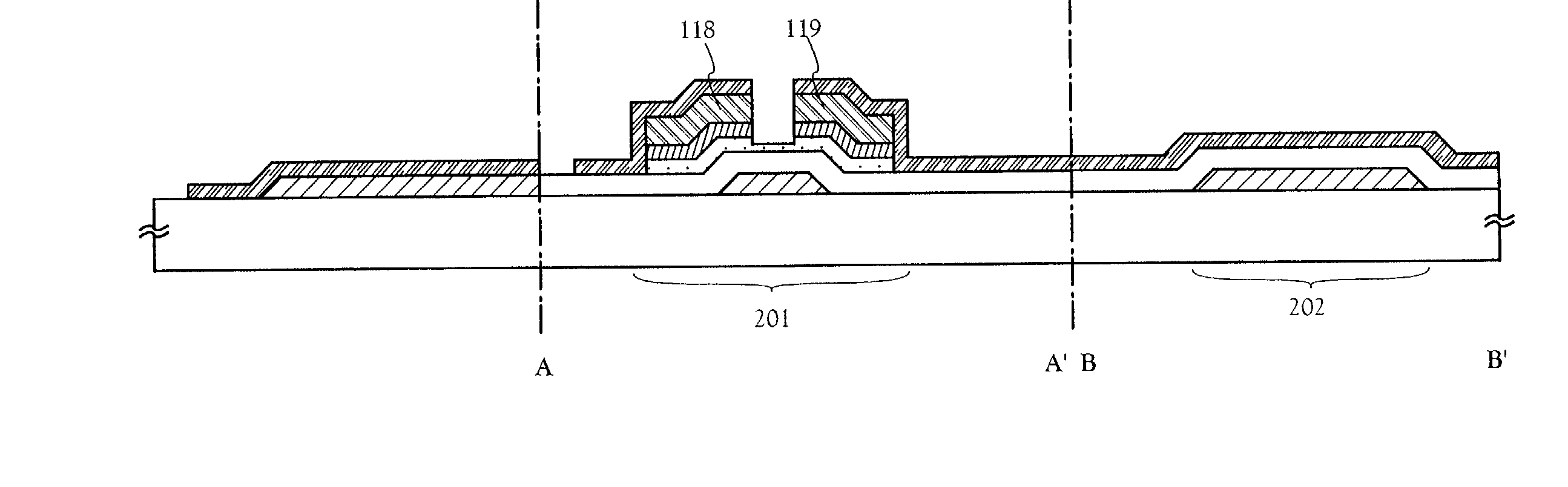
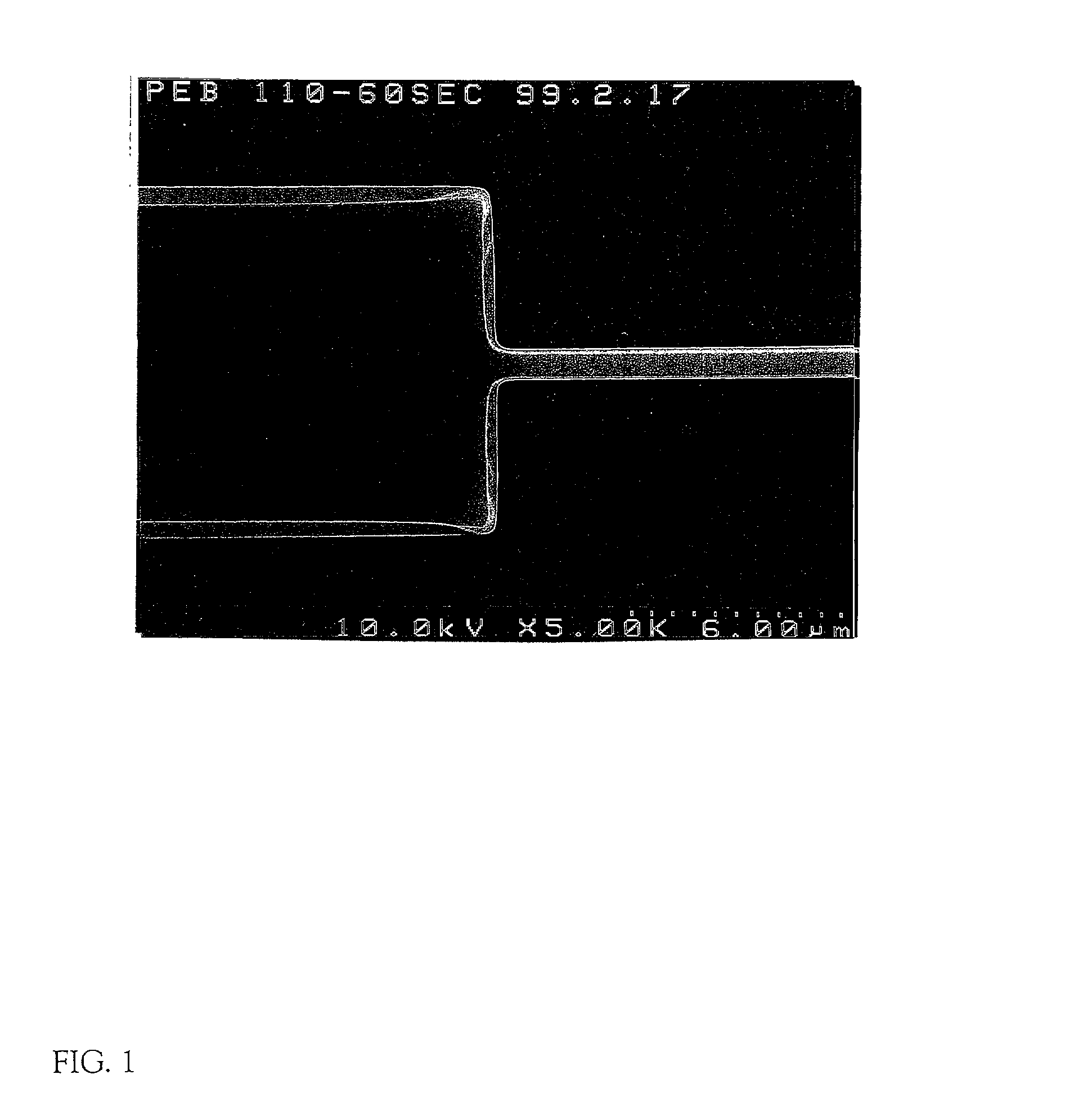
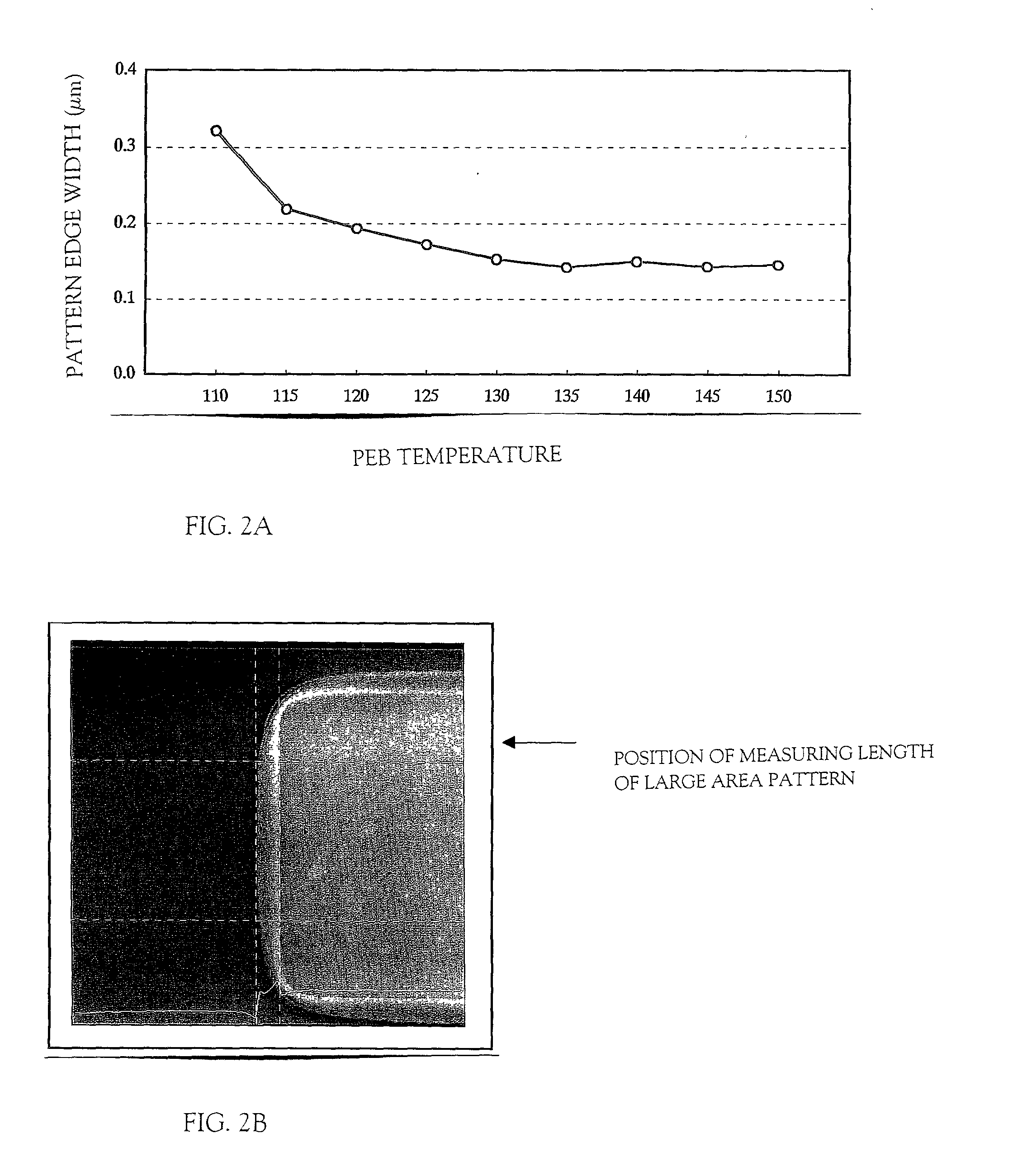
[0051] The present invention relates to a structure of an inverted stagger type TFT having a bottom gate structure and a method of manufacturing the same, characterized in that, by restricting a bake condition between a pre-bake temperature or PEB temperature and a post-bake temperature in a photolithography step, taper angles of various dimensions of resist patterns are accurately controlled, as a result, accurately controlling shapes of various dimensions of etching patterns. Specific embodiment mode of the structure of the inverted stagger type TFT and the method of manufacturing the same in accordance with the present invention are described below with reference to FIGS. 4A-4D, FIGS. 5A-5B and FIG. 6.

[0052] It is to be noted that FIGS. 4A-4D and FIGS. 5A-5B are cross-sectional views illustrating a manufacturing steps of an active matrix liquid crystal display device, and FIG. 6 is a top view illustrating configuration of a pixel region in the active matrix liquid crystal displa...


PUM


Abstract

In a patterning process of a semiconductor device having inverted stagger type TFTs, a normal photolithography step using diazo naphthoquinone (DNQ)-Novolac resin based positive photo resist is applied, and a problem of the area dependency of the photo resist pattern side wall taper angle may occur. The problem is critical for the reason of influence on variation of an etching shape in a dry-etching step. The present invention has an object to solve the above problem. In a photolithography step, which is patterning step of a semiconductor device having inverted stagger type TFTs, by adjusting a pre-bake temperature or a PEB (post-exposure-bake) temperature, and positively performing evacuation of solvent in a state of a photo resist film, the volume contraction by evacuation of solvent at the post-bake is reduced, and the problem of the area dependency of the photo resist pattern side wall taper angle is solved, which is deformation due to the volume contraction.

Description

TECHNICAL FIELD TO WHICH THE INVENTION BELONGS[0001] The present invention relates to a semiconductor device having a circuit formed of thin film transistors (thereafter, referred to as TFTs) and a method of manufacturing the same. The semiconductor device includes, for example, an electro-optical device such as a liquid crystal display formed of TFTs.[0002] More specifically, the present invention relates to a method of manufacturing a semiconductor device having inverted staggered type TFTs with a bottom gate structure, and more particularly to a photolithography for patterning the semiconductor device.PRIOR ART[0003] In recent years, an active matrix liquid crystal display technology using TFTs is of great interest. Since an active matrix display is provided with a TFT switch on each pixel, a liquid crystal orientation state of TN (i.e., twisted nematic) mode is available, and it is advantageous in terms of response speed, viewing angle and contrast, compared with a passive matri...

Claims


Application Information

Patent Timeline
IPC IPC(8): H01L21/336
CPCH01L29/66765G02F1/13439G02F1/136286
Inventor UEHARA, ICHIROTOSHIMA, KAZUHIROYAMAZAKI, SHUNPEI
Owner SEMICON ENERGY LAB CO LTD
Why Eureka
Try Eureka