Method of forming a metal gate

Inactive Publication Date: 2002-09-12
SAMSUNG ELECTRONICS CO LTD
View PDF0 Cites 52 Cited by
  • Summary
  • Abstract
  • Description
  • Claims
  • Application Information

AI Technical Summary

Benefits of technology

0013] In the preferred embodiment, nitrogen gas or argon gas

Problems solved by technology

As the integration level of semiconductor devices increases, the conventional polysilicon gate electrode fails to meet a suitable operation speed and an adequate sheet resistance for the gate electrode.
Unfortunately, the tungsten is easily oxidized, which results in abnormal oxidation that

Method used


Image

  • Method of forming a metal gate
  • Method of forming a metal gate
  • Method of forming a metal gate

Examples


Example

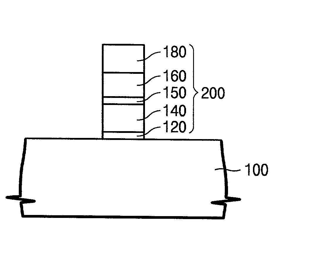
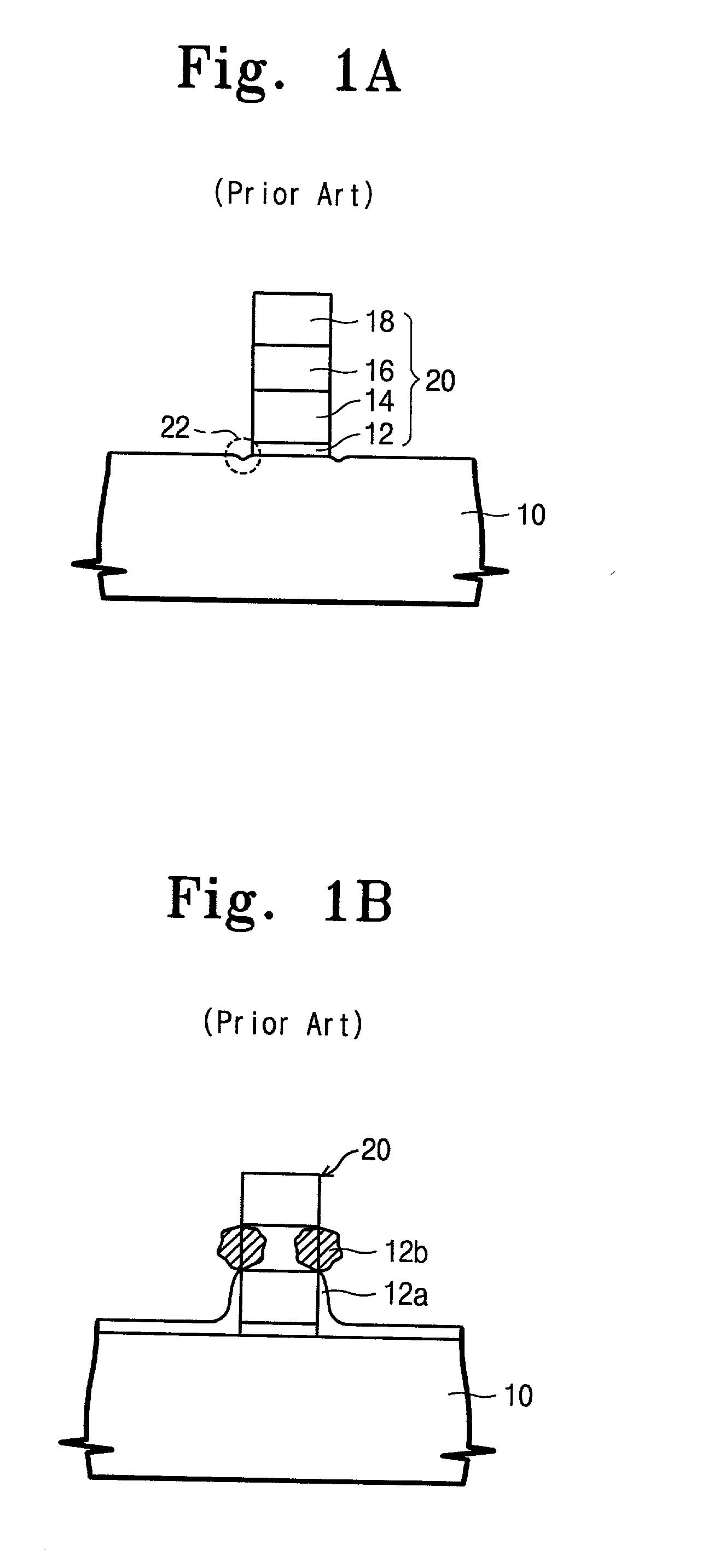
[0022] A new and improved method of forming a metal gate will now be described more fully with reference to attached drawings. The description of conventional processing steps (e.g., device isolation, well formation, and ion implantation) will not be repeated in the present discussion.

[0023] Referring now to FIG. 3A, a gate insulating layer 120 is formed on a semiconductor substrate 100 using a conventional technique such as thermal oxidation or chemical vapor deposition (CVD). A polysilicon layer 140, a barrier metal layer 150, a metal layer 160, and a gate capping layer 180 are sequentially formed as gate electrode materials. The barrier metal layer 150, the metal layer 160, and the gate capping layer 180 may comprise, for example, tungsten nitride, tungsten, and silicon nitride, respectively. The barrier metal layer 150 prevents the polysilicon layer 140 from reacting with the metal layer 160. The metal layer 160 may be made of a high melting point metal except tungsten, and the ...


PUM


Abstract

In a method of forming a metal gate electrode, an annealing process is performed in a hydrogen-containing gas ambient following a selective oxidation process. During the annealing process, a metal oxide layer formed by the selective oxidation process is removed by a reduction reaction or hydrogen atoms are contained in the metal oxide layer to suppress whisker nucleation and surface mobility.

Description

[0001] This application relies for priority upon Korean Patent Application No. 2001-12600, filed on Mar. 12, 2001, the contents of which are herein incorporated by reference in their entirety.FIELD OF THE INVENTION[0002] The present invention relates to a method of manufacturing a semiconductor device and, more particularly, to a method of forming a metal gate.BACKGROUND OF THE INVENTION[0003] In a semiconductor fabrication process, a gate electrode of a MOS transistor is formed by etching a conductive layer that is formed on a semiconductor substrate to a predetermined thickness. Conventionally, polysilicon is used as a gate electrode material. This is because the polysilicon has excellent interfacial characteristics with respect to a gate oxide layer at high temperatures. As the integration level of semiconductor devices increases, the conventional polysilicon gate electrode fails to meet a suitable operation speed and an adequate sheet resistance for the gate electrode. Therefore...

Claims


Application Information

Patent Timeline
IPC IPC(8): H01L21/336H01L21/28H01L29/423H01L29/43H01L29/49H01L29/78
CPCH01L21/28061H01L21/28247H01L21/18
Inventor CHO, MAHN-HOKU, JA-HUMCHOI, CHUL-JOONCHO, JUN-KYUHEO, SEONG-JUN
Owner SAMSUNG ELECTRONICS CO LTD
Why Eureka
Try Eureka