
Modular imaging apparatus

a module imaging and apparatus technology, applied in the field of imaging apparatus, can solve the problems of limiting the maximum size of monolithic detectors to a few square centimeters, unable to recover lost information, and not being able to address the replacement of components

Inactive Publication Date: 2002-09-19
SIMAGE
View PDF0 Cites 31 Cited by
  • Summary
  • Abstract
  • Description
  • Claims
  • Application Information

AI Technical Summary

Benefits of technology

[0021] This enables a modular arrangement of a plurality of tiles such that the tiles can be readily arranged with respect to one another and whereby the modules may be assembled with respect to one another to provide a large area imaging apparatus. The imaging apparatus according to the invention also provides a basis for simplifying the connection to and arrangement of circuit components external to the imaging devices as will be explained below with respect to preferred developments of the invention.
[0023] Preferably, the tiles are mounted on the modules in a removable manner to facilitate the replacement of faulty tiles when required and / or the replacement of tiles having different resolutions and / or specifications for different imaging applications. Preferably, the modules are also mounted on the support structure in a removable manner permitting easy replacement of a complete module when required and / or the replacement of modules carrying tiles having different resolutions and / or specifications for different imaging applications.
[0025] In a preferred embodiment, a module comprises a board comprising, on a first surface thereof, an array of tile mounting locations, each mounting location comprising an arrangement of mounting location contacts for contacting corresponding tile contacts on a tile. The board is elongate and comprises two or more rows of mounting locations for supporting two or more rows of tiles. The board has, on the first surface, a circuit region not populated with the tiles. Preferably, the circuit region is adjacent one end of the board to maximise the size available for the imaging array. The circuit region can comprises control circuitry for controlling access to and output of signals from the imaging devices. Alternatively, or in addition, circuitry can be provided on a surface of the board, opposite to the first surface.
[0026] Thus, the module can comprises a board, for example a multilayer printed circuit board, having a first area with tile mounting locations and a second area for circuitry external to the tiles, including, for example, power supply circuitry, module controller circuitry and external interface circuitry. Preferably, the board is a multilayer printed circuit board, conductive tracks connecting the mounting location contacts to the circuitry. The provision of the circuitry in a predefined area of the module enhances the modularity of the apparatus and allows the tailoring of the detail design to suit particular applications and technologies.
[0027] In a preferred arrangement to enhance the performance of communications between the individual tiles and an external computer, tiles within a module are electrically grouped in clusters. Tiles within a cluster are preferably read out in series and one or more clusters are also readout in series, thus effectively forming larger clusters, termed megaclusters. In a preferred embodiment the megaclusters are read out in parallel. Advantageously, some of the clusters can be selectively de-activated, so that a megacluster can comprise fewer tiles, where it is desired to increase read out speed and smaller areas need to be imaged. In one embodiment, the outputs of the megaclusters of one module are multiplexed on the module so as to provide one output per module. Alternatively, or in addition, the outputs from different modules can be multiplexed in order to further reduce the overall number of signals to be digitized.
[0034] An embodiment of the invention can enable, for example, the provision of an imaging cassette having a total imaging area of, say, approximately 100.times.200 mm and a thickness of 2.5 cm or less. The cassette can be portable and lightweight. Also defective tile replacement can be facilitated. Given a pixel size of 35 micrometers, an imaging cassette of 100.times.200 mm could comprise about 16 million pixels. Pixel digitisation with 10 or 12 bits resolution can be provided by 16 bits of computer memory per pixel. Fast data transfer from cassette to computer can be achieved, for example with a data transfer time of less than 5 seconds.

Problems solved by technology

However, limitations on ASIC CMOS technology (e.g. yield) limit the maximal size of monolithic detectors to a few square centimeters.
The major challenge is the formation of a large continuous imaging area without any blind regions.
However, this method does not recover lost information but only provides an approximation.
Furthermore, as individual detectors are rigidly glued on the apparatus defective component replacement is not addressed.
Although the total thickness of the apparatus is independent of the imaging area, the overall structure is, once again, rigid and does not allow for simple individual detector replacement.
However, individual mounting of the individual tiles is required, which can be a time consuming and difficult task for large arrays.
Also, providing large numbers of electrical connections to the individual tiles for a large array can require the development of expensive support planes.
Accordingly, there remain problems to be solved regarding the large area imaging, such as facilitating the accurate relative positioning of large numbers of individual tiles on the support plane.

Method used


Image

  • Modular imaging apparatus
  • Modular imaging apparatus
  • Modular imaging apparatus

Examples


Embodiment Construction

[0058] Exemplary embodiments of the invention are described hereinafter, by way of example only, with reference to the accompanying drawings.

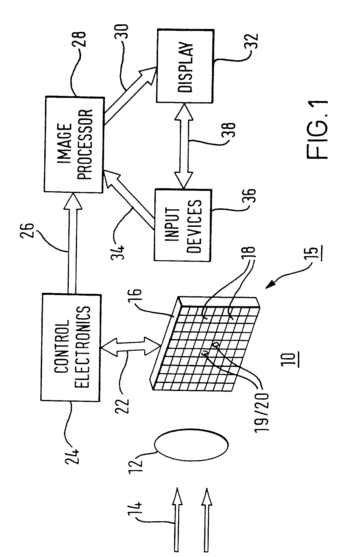
[0059] FIG. 1 is a schematic representation of an example of an imaging system 10 as described in the Applicant's International application WO 95 / 33332 for radiation imaging of an object 12 subjected to radiation 14. The radiation may, for example, be X-ray radiation and the object 12 may, for example, be a part of a human body. The imaging device comprises an imaging array 15 including at least one Active-pixel Semiconductor Imaging Devices (ASID) 16. Although only one ASID 16 is shown schematically in FIG. 1, the imaging array will typically include a plurality of imaging devices 16. Each imaging device provides a plurality of image, or pixel cells 18. Each imaging device directly detects high energy incident radiation such as X-rays, .gamma.-rays, .beta.-rays or .alpha.-rays and accumulates at each pixel cell, by means of a randomly accessib...


PUM


Abstract

Radiation imaging apparatus includes a support structure for a number of modules which each in their turn support a number of imaging device tiles. An imaging device on each tile provides an array of radiation detector cells. With the modular construction, the apparatus can provide a large imaging array from a large number of individual tiles. The support structure may be located in or form part of an imaging cassette. The modules provide tile mounting locations in one or more rows for the imaging device tiles, whereby the tiles may be accurately mounted with respect the module and to each other prior to being mounted on the support structure. The tiles are mounted on the modules and the modules are mounted within the cassette in a removable manner to facilitate the replacement of faulty tiles when required and / or the replacement of tiles having different resolutions and / or specifications for different imaging applications. Various arrangements for electronically clustering tiles are provided.

Description

[0001] This is a continuation of application Ser. No. 09 / 197,606 filed Nov. 23, 1998.[0002] The invention relates to imaging apparatus having a modular structure. In particular the invention relates to imaging apparatus comprising a plurality of imaging devices.BACKGROUND TO INVENTION[0003] The invention finds application to imaging apparatus for large area imaging using semiconductor imaging devices and is particularly suitable for high energy radiation imaging (i.e. radiation having energies in excess of 1 keV, such as X-rays).[0004] Traditional arrangements for X-ray imaging, including cassette film, other modalities such as wire chambers, scintillating crystals or screens, (e.g. Sodium Iodide Nal), BGO (Bismuth Gerranium Oxide) and CR plates (Computed Radiography), have been utilized over the past forty years.[0005] More recently, semiconductor imaging devices have been employed, including CCD-based devices, both in stand-alone implementations and coupled to scintillating screen...

Claims


Application Information

Patent Timeline
Patent Type & Authority Applications(United States)
IPC IPC(8): H04N5/335G01T1/24H01L31/09H01L27/14H04N5/32H04N5/225H04N25/00
CPCH04N5/379G01T1/243H04N25/79
Inventor KYYHKYNEN, ARTO
Owner SIMAGE
Learn More