Doped elongated semiconductors, growing such semiconductors, devices including such semiconductors and fabricating such devices

a technology of semiconductors and long semiconductors, applied in the field of nanometer-scale semiconductor devices, can solve the problems of high cost and need a clean room in the typical state-of-the-art semiconductor fabrication facility

Inactive Publication Date: 2002-09-19
PRESIDENT & FELLOWS OF HARVARD COLLEGE
View PDF98 Cites 626 Cited by
  • Summary
  • Abstract
  • Description
  • Claims
  • Application Information

AI Technical Summary

Benefits of technology

0043] In various aspects of this embodiment, the device comprises one or more of the following:. a switch; a diode; a Light-Emitting Diode; a tunnel diode; a Schottky diode; a Bipolar Junction Transistor; a Field Effect Transistor; an inverter; a complimentary inverter; an optical sensor; a sensor for an analyte (e.g., DNA); a memory device; a dynamic memory device; a static memory device; a laser; a logic gate; an AND gate; a NAND gate; an EXCLUSIVE-AND gate; an OR gate; a NOR gate; an EXCLUSIVE-OR gate; a latch; a register; clock circuitry; a logic array; a state machine; a programmable circuit; an am...

Problems solved by technology

Typical state-of-the-art semiconductor fabrication facilities involve relatively hig...

Method used


Image

  • Doped elongated semiconductors, growing such semiconductors, devices including such semiconductors and fabricating such devices
  • Doped elongated semiconductors, growing such semiconductors, devices including such semiconductors and fabricating such devices
  • Doped elongated semiconductors, growing such semiconductors, devices including such semiconductors and fabricating such devices

Examples


examples

[0245] Doping and Electrical Transport in Nanowires

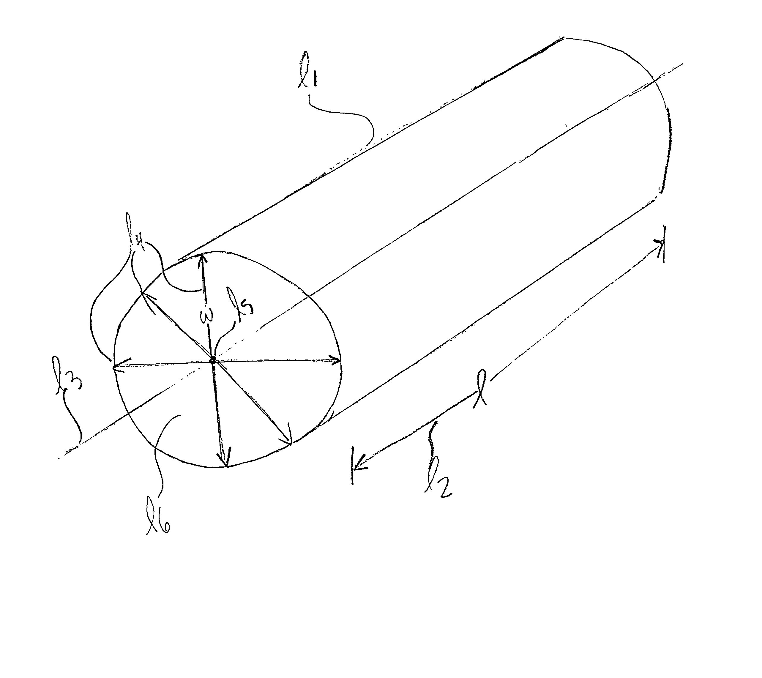
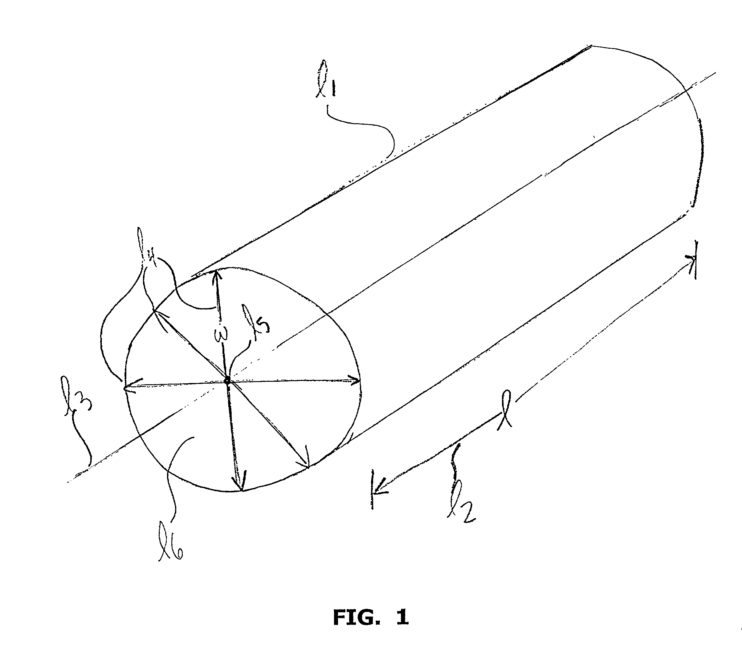
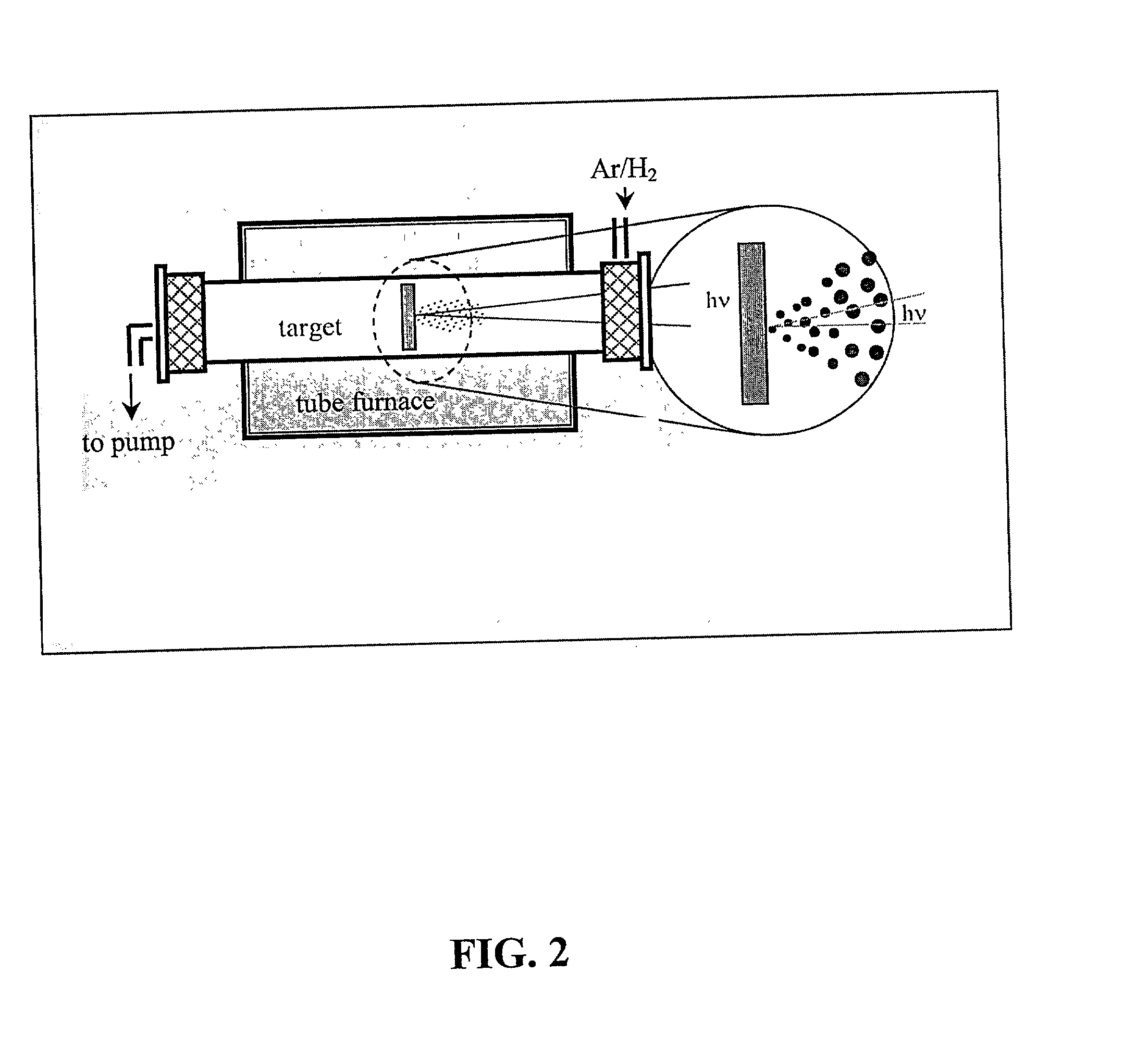
[0246] Single crystal n-type and p-type silicon nanowires (SiNWs) have been prepared and characterized by electrical transport measurements. As used herein, a "single crystal" item is an item that has covalent bonding, ionic bonding, or a combination thereof throughout the item. Such a single crystal item may include defects in the crystal, but is distinguished from an item that includes one or more crystals, not ionically or covalently bonded, but merely in close proximity to one another. Laser catalytic growth was used to introduce controllably either boron or phosphorous dopants during the vapor phase growth of SiNWs. Two terminal, gate-dependent measurements made on individual boron-doped and phosphorous-doped SiNWs show that these materials behave as p-type and n-type materials, respectively. Estimates of the carrier mobility made from gate-dependent transport measurements are consistent with diffusive transport. In addition, t...


PUM

PropertyMeasurementUnit
Timeaaaaaaaaaa
Widthaaaaaaaaaa
Widthaaaaaaaaaa

Abstract

A bulk-doped semiconductor that is at least one of the following: a single crystal, an elongated and bulk-doped semiconductor that, at any point along its longitudinal axis, has a largest cross-sectional dimension less than 500 nanometers, and a free-standing and bulk-doped semiconductor with at least one portion having a smallest width of less than 500 nanometers. Such a semiconductor may comprise an interior core comprising a first semiconductor; and an exterior shell comprising a different material than the first semiconductor. Such a semiconductor may be elongated and my have, at any point along a longitudinal section of such a semiconductor, a ratio of the length of the section to a longest width is greater than 4:1, or greater than 10:1, or greater than 100:1, or even greater than 1000:1. At least one portion of such a semiconductor may a smallest width of less than 200 nanometers, or less than 150 nanometers, or less than 100 nanometers, or less than 80 nanometers, or less than 70 nanometers, or less than 60 nanometers, or less than 40 nanometers, or less than 20 nanometers, or less than 10 nanometers, or even less than 5 nanometers. Such a semiconductor may be a single crystal and may be free-standing. Such a semiconductor may be either lightly n-doped, heavily n-doped, lightly p-doped or heavily p-doped. Such a semiconductor may be doped during growth. Such a semiconductor may be part of a device, which may include any of a variety of devices and combinations thereof, and, and a variety of assembling techniques may be used to fabricate devices from such a semiconductor. Two or more of such a semiconductors, including an array of such semiconductors, may be combined to form devices, for example, to form a crossed p-n junction of a device. Such devices at certain sizes may exhibit quantum confinement and other quantum phenomena, and the wavelength of light emitted from one or more of such semiconductors may be controlled by selecting a width of such semiconductors. Such semiconductors and device made therefrom may be used for a variety of applications.

Description

RELATED APPLICATIONS[0001] This application claims priority under 35 U.S.C. .sctn.119(e) to commonly-owned, co-pending U.S. Provisional Patent Application Serial No. 60 / 226,835, entitled, "Semiconductor Nanowires", filed Aug. 22, 2000; Serial No. 60 / 292,121, entitled, "Semiconductor Nanowires", filed May 18, 2001; Serial No. 60 / 254,745, entitled, "Nanowire and Nanotube Nanosensors," filed Dec. 11, 2000; Serial No. 60 / 292,035, entitled "Nanowire and Nanotube Nanosensors," filed May 18, 2001; Serial No. 60 / 292,045, entitled "Nanowire Electronic Devices Including Memory and Switching Devices," filed May 18, 2001; and Serial No. 60 / 291,896, entitled "Nanowire Devices Including Emissive Elements and Sensors," filed May 18, 2001, each of which is hereby incorporated by reference in its entirety.FIELD OF THE INVENTION[0002] The present invention relates generally to sub-microelectronic semiconductor devices, and more particularly to nanometer-scale semiconductor articles, for example, nano...

Claims


Application Information

Patent Timeline
IPC IPC(8): C30B11/00H01L29/73C30B25/00G01N27/12G01N27/414G01N33/543G11C13/02H01L21/329H01L21/331H01L23/532H01L27/10H01L29/06H01L29/207H01L29/267H01L29/88H01L33/06H01L33/18H01L51/00H01L51/30
CPCB01J23/50B01J23/52B01J23/72B01J35/0013B01J37/349B81C1/0019B81C1/00206B82Y10/00B82Y15/00B82Y30/00B82Y40/00C30B11/00C30B25/005G01N27/4146G01N33/54373G11C13/0014G11C13/0019G11C13/025G11C13/04G11C2213/77G11C2213/81H01L21/02521H01L21/02532H01L21/0254H01L21/02543H01L21/02557H01L21/0256H01L21/02573H01L21/02581H01L21/02603H01L21/02606H01L21/0262H01L21/02628H01L21/02631H01L21/02636H01L21/02639H01L21/02645H01L21/02653H01L23/53276H01L29/045H01L29/0665H01L29/0673H01L29/068H01L29/16H01L29/1602H01L29/18H01L29/20H01L29/207H01L29/22H01L29/24H01L29/26H01L29/267H01L33/06H01L33/18H01L33/20H01L51/002H01L51/0048C30B29/605Y10S977/892Y10S977/762Y10S977/847Y10S438/962Y10S977/936Y10S977/882Y10S977/883Y10S977/858Y02E10/549H01L2924/0002H01L2924/00Y10T428/24Y02P70/521H10K71/30H10K85/221H01L21/18Y02P70/50
Inventor LIEBER, CHARLES M.CUI, YIDUAN, XIANGFENGHUANG, YU
Owner PRESIDENT & FELLOWS OF HARVARD COLLEGE
Why Eureka
Try Eureka