Method and apparatus for electromagnetic powder deposition
a technology of electromagnetic powder and method, applied in the direction of molten spray coating, plasma technique, coating, etc., can solve the problems of inconvenient electrolytic plating, material difficulty, and limitations of electrolytic plating process
- Summary
- Abstract
- Description
- Claims
- Application Information
AI Technical Summary
Problems solved by technology
Method used
Image
Examples
embodiment 180
[0086] FIG. 9 illustrates the recharge circuit 176 that employs a recharge capacitor bank 182 and a charging inductor 184 to power and regulate the recharge cycles. A bank of bipolar transistors (IGBT) 186 having isolated-gates controls the current flow from the recharge capacitor 182 to the charging inductor 184. The collectors and emitters of the IGBT's 186 are connected in series. A series bank of silicon controlled rectifiers (SCR's) 188 insures that the charging current from the recharge capacitor bank 182 does not pass through the PFN 160 by having symmetrical voltage holdoff. The bank of IGBT's 186, the bank of SCR's 188, and the control switch 174 each have separate switch blocks 190, 192, 194. The switch blocks 190, 192, 194 provide gate signals in response to optical signals from the controller block 196. The control module 178 also includes a sensor block 198 to shut the PFN 160 and / or the recharge circuit 176 down in response to preselected types of errors. One preselect...
embodiment 220
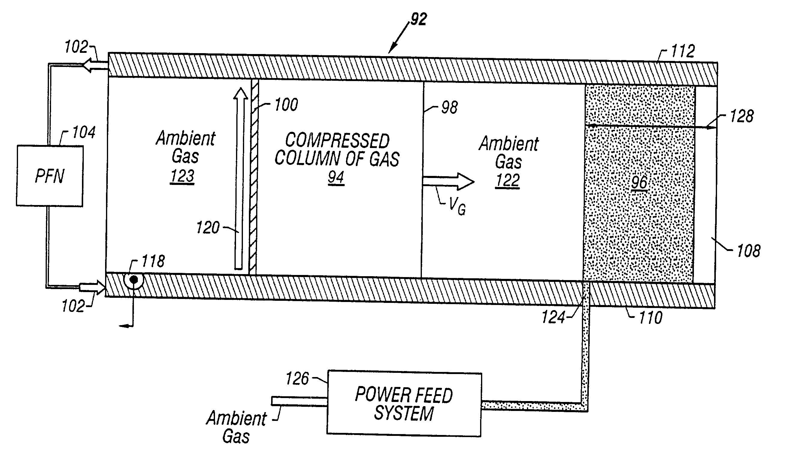
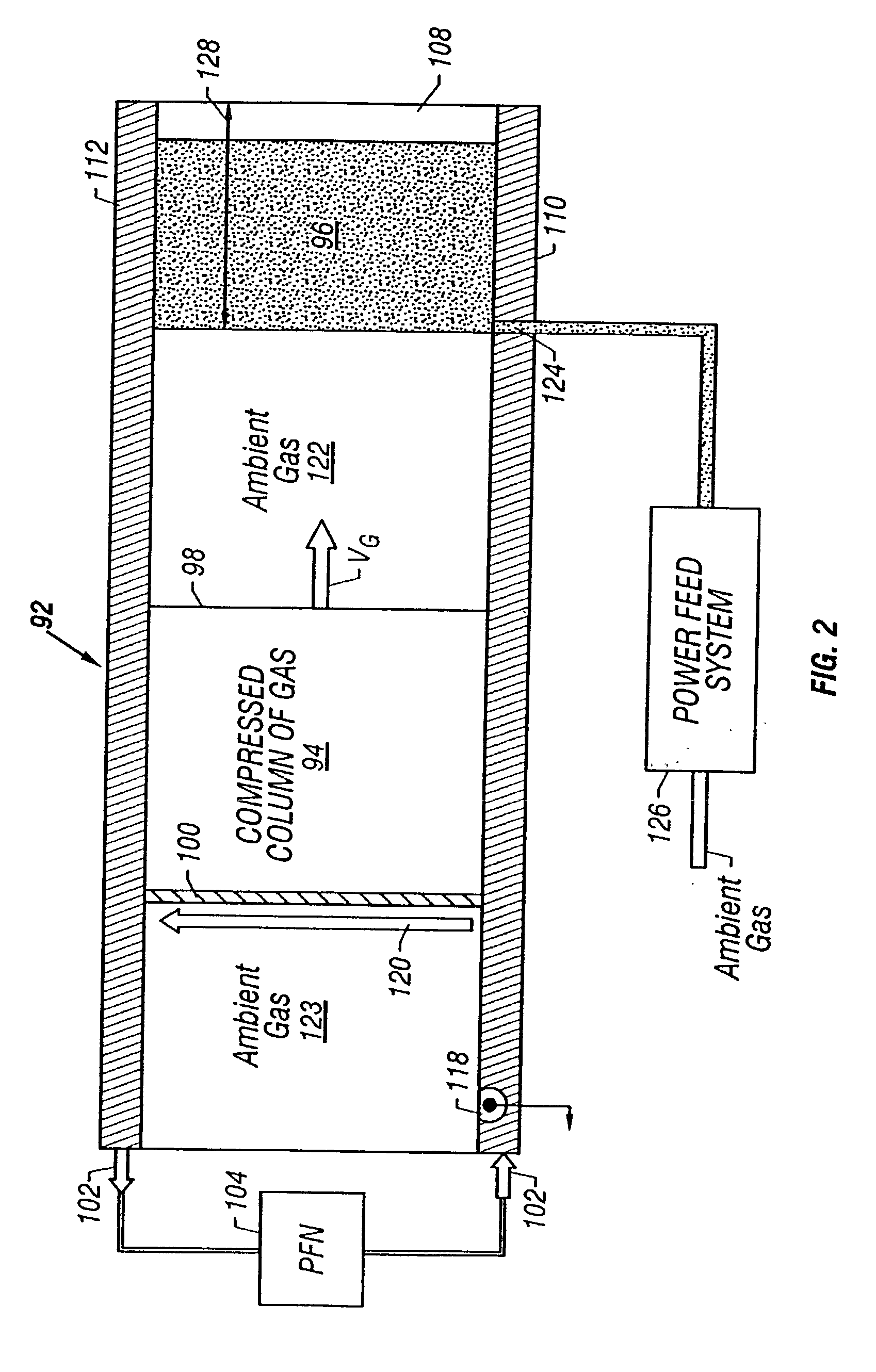
[0091] FIG. 11A illustrates an embodiment 220 for the arc initiator 118 for the plasma armature 100 of FIG. 2. The arc initiator 220 has a coaxial geometry that includes a solid wire electrode 221 that is centered in a cavity 222 having a circular cross section. The cavity 222 is filled with the ambient gas 123 that fills a portion of the railgun 92 of FIGS. 2 and 4. The cavity 222 has a narrow slit 223 that opens along the full width of the bore 108 of the first conducting rail 110 of FIGS. 2-4. In one embodiment, the wire electrode 221 is made of tungsten, the cavity 222 is about 3 millimeters in diameter, and the slit 223 is about 1 millimeter in width. A high-frequency signal generator 224 powers the arc initiator 220 through a first lead 225 connected to the wire electrode 221 and a second lead 230 connected to the conducting rail 110.
[0092] FIG. 11B illustrates one embodiment of the high-frequency signal generator 224 of FIG. 11A. A radio frequency (RF) amplifier 226, e.g., a ...
PUM
| Property | Measurement | Unit |
|---|---|---|
| diameter | aaaaa | aaaaa |
| frequency | aaaaa | aaaaa |
| velocities | aaaaa | aaaaa |
Abstract
Description
Claims
Application Information


