GaN HBT superlattice base structure

a superlattice base structure and transistor technology, applied in the direction of basic electric elements, electrical equipment, semiconductor devices, etc., can solve the problems of reducing the output power of the device, reducing the efficiency of the device, and a lower frequency of operation

Inactive Publication Date: 2002-10-17
NORTHROP GRUMAN CORP
View PDF1 Cites 32 Cited by
  • Summary
  • Abstract
  • Description
  • Claims
  • Application Information

AI Technical Summary

Problems solved by technology

The injection of holes into the base layer results in a lower cut off frequency and lower current gain of the device resulting in lower efficiency and a lower frequency of operation of the device.
Unfortunately, such a configuration results in a base layer with more resistance which, in turn, reduces the output power of the device.

Method used


Image

  • GaN HBT superlattice base structure
  • GaN HBT superlattice base structure

Examples


Embodiment Construction

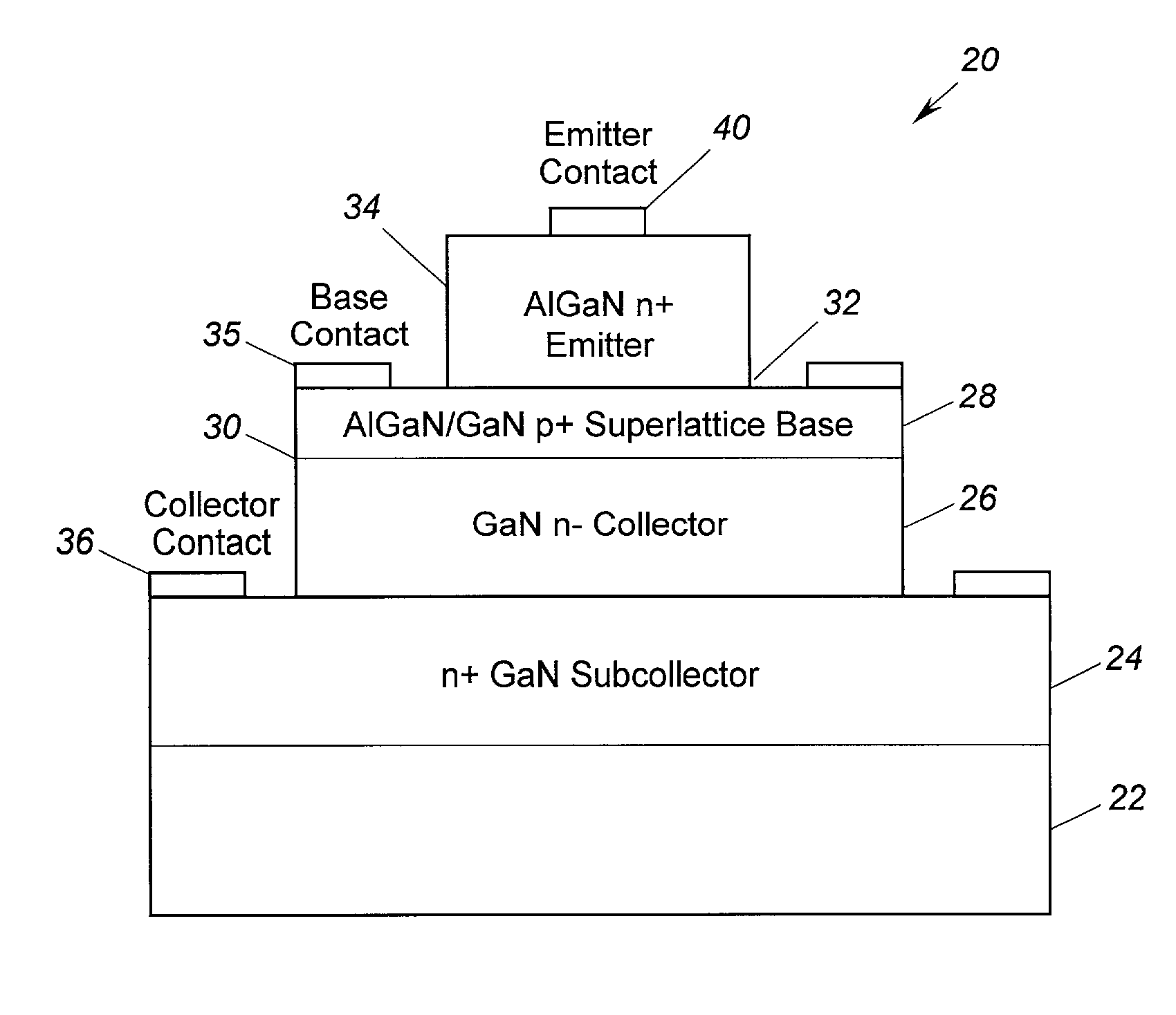
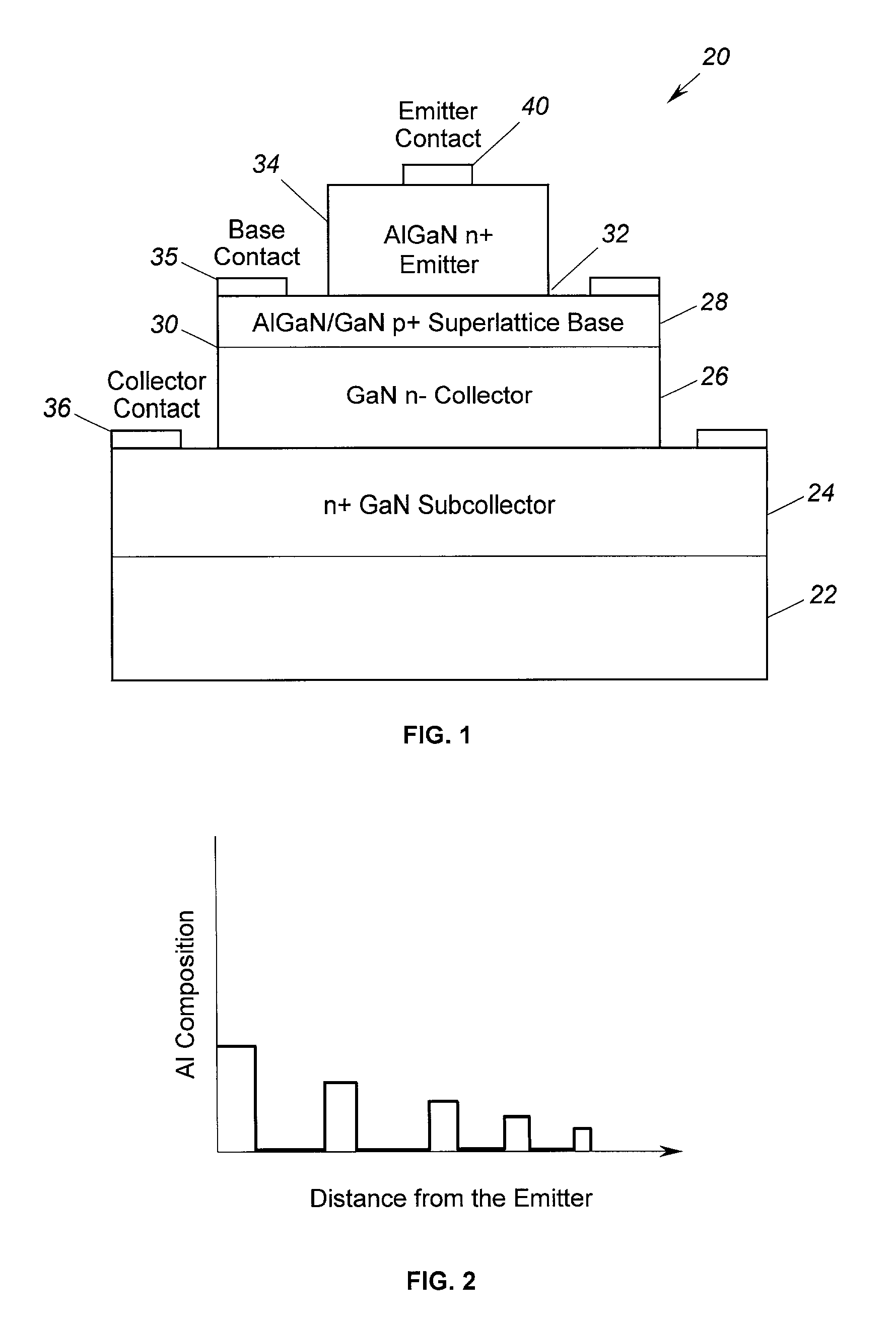
[0014] The present invention relates to a heterojunction bipolar transistor (HBT) with improved base transit time and increased p-type carrier concentration in the base which provides for higher efficiency power operation and higher frequency operation. In HBTs formed from gallium nitride / aluminum gallium nitride (GaN / AlGaN) material systems, the p-type carrier concentration is limited by high acceptor activation energies. The present invention utilizes alternating layers of GaN and AlGaN to form a graded superlattice which effectively increases the p-type carrier concentration by effectively reducing the activation energy. Higher p-type carrier concentration allows for higher efficiency power operation and high frequency operation. The graded superlattice results in the band gap energy across the base being graded. The grading induces an electrostatic field across the base which increases the carrier velocity which reduces the carrier transit time. For example, for the configuratio...


PUM

PropertyMeasurementUnit
thicknessaaaaaaaaaa
thicknessaaaaaaaaaa
thicknessaaaaaaaaaa

Abstract

A heterojunction bipolar transistor (HBT) (20) with alternating layers of gallium nitride (GaN) and aluminum gallium nitride (AlGaN) with varying Al composition forming a graded superlattice structure in the base layer (28) includes. The thin layers of AlGaN in the base layer (28) increases the base p-type carrier concentration. Grading of the Al composition in the thin AlGaN layers induces an electrostatic field across the base layer (28) that increases the carrier velocity and reduces the carrier transit time. The structure thus decreases the transit time and at the same time increases the p-type carrier concentration to improve the operating efficiency of the device.

Description

[0001] 1. Field of the Invention[0002] The present invention relates to a heterojunction bipolar transistor (HBT) and more particularly to an HBT and method for making an HBT having higher efficiency and higher frequency operation without the fabrication complexities of known HBTs.[0003] 2. Description of the Prior Art[0004] Heterojunction bipolar transistors (HBT) are generally known in the art. Examples of such devices are disclosed in U.S. Pat. Nos. 5,349,201; 5,365,077; 5,404,025 and commonly owned U.S. Pat. No. 5,448,087 and 5,672,522, all hereby incorporated by reference. Such HBTs are known to be used in applications requiring relatively high frequency response and wider temperature range of operation and are used, for example, in power amplifiers, low noise amplifiers and power conversion electronic circuits in satellite and solar applications.[0005] Typical HBT's are normally formed on a semiconducting substrate, such as gallium arsenide (GaAs) or Indium phosphide (InP). Co...

Claims


Application Information

Patent Timeline
Patent Type & Authority Applications(United States)
IPC IPC(8): H01L21/331H01L29/15H01L29/20H01L29/737
CPCH01L29/155H01L29/7371H01L29/2003
Inventor WOJTOWICZ, MICHAEL
Owner NORTHROP GRUMAN CORP
Why Eureka
Try Eureka