Thermoelectric module and method of producing the same

a technology of thermoelectric modules and soldering agents, which is applied in the manufacture/treatment of thermoelectric devices, lighting and heating apparatus, and the details of the semiconductor/solid-state device to be heated, etc., and can solve the problems of low connection reliability at the connection of the structure to be heat-radiated, including pb, and environmental degradation, and no other soldering agent makes it possible to produce the thermoelectric module at a lower cos

Inactive Publication Date: 2002-10-17
AISIN SEIKI KK
View PDF2 Cites 8 Cited by
  • Summary
  • Abstract
  • Description
  • Claims
  • Application Information

AI Technical Summary

Problems solved by technology

However, using the above-mentioned soldering agent which is lower in melting point (solidus / liquidus) than the soldering agent which is used in the module assembly for the connection of the semiconductor tip can lower the connection reliability at the connection of the structure to be heat-radiated when the module is required to be used in a severe thermal environment.
In addition, if 95Sn5Sb soldering agent is employed as the soldering agent which is used in the module assembly for the connection of semiconductor tip, making the other soldering agent as high as possible in heat resistance results in including Pb, which is environmentally unacceptable.
In addition, no other soldering agents make it possible to produce the thermoelectric module at a lower cost.

Method used


Image

  • Thermoelectric module and method of producing the same
  • Thermoelectric module and method of producing the same

Examples


Embodiment Construction

[0027] Hereinafter, embodiments of the present invention will be described in detail with reference to the attached drawings.

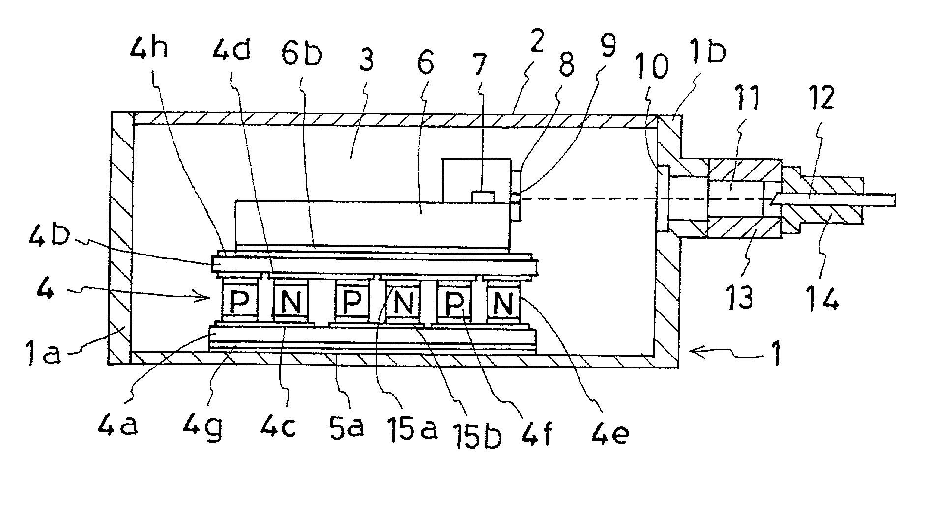
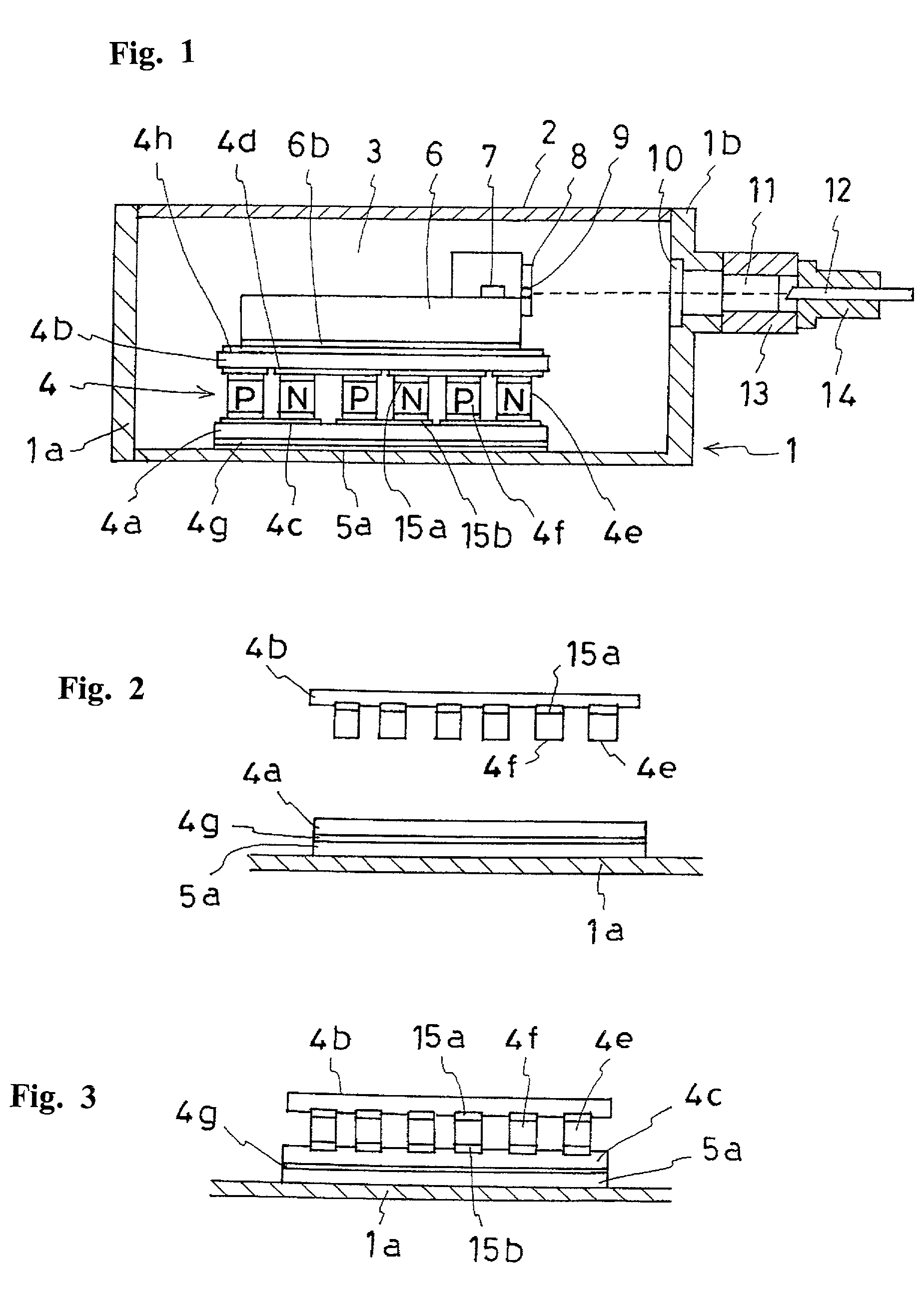
[0028] Referring first to FIG. 1, there is illustrated a semiconductor laser module in accordance with an embodiment of the present invention. The semiconductor laser module includes a sealed or fluid-tight package 3 which is constituted by a box-shaped case 1 and a cover 2 covering the case 1. An amount of dried nitrogen gas is filled in the sealed package 3. On an inside surface of a bottom wall 1a of the case 1, there is soldered by a first soldering layer (i.e., a soldering layer between the case and heat-radiation side insulating substrate) 5a, via a second lower electrode 4g, an insulating substrate (i.e. heat-radiation side insulating substrate) 4a of a Peliter element type thermoelectric module 4 for controlling the thermoelectric module 4.

[0029] In the thermoelectric module 4, the heat-radiation side insulating substrate 4a is opposite to a heat-absor...


PUM

PropertyMeasurementUnit
temperatureaaaaaaaaaa
Temperatureaaaaaaaaaa
temperatureaaaaaaaaaa

Abstract

A thermoelectric module which includes a case 1, a heat-radiation side insulating substrate 4a, a heat-absorption side insulating substrate 4b, a first soldering layer 5a formed of a first soldering agent to connect the heat-radiation side insulating substrate 4a and the case 1, a plurality of P-type and N-type semiconductor chips interposed between the heat-radiation side insulating substrate 4a and the heat-absorption side insulating substrate 4b, the plurality of P-type and N-type semiconductor chips being arranged alternately, and a second soldering layer 15a (15b) formed of a second soldering agent to connect the heat-radiation side insulating substrate 4a and one end of each of the plural P-type and N-type semiconductor chips (the heat-absorption side insulating substrate 4b and the other end of each of the plural P-type and N-type semiconductor chips), the first soldering agent and the second soldering agent being identical in raw material.

Description

[0001] The present application is based on and claims priority under 35 U.S.C. .sctn.119 with respect to Japanese Patent Application No.2001-022565 filed on Jan. 31, 2001 (13th Year of Heisei), the entire content of which is incorporated herein by reference.[0002] 1. Field of the Invention[0003] The present invention is generally directed to a thermoelectric module and method of producing the same, the thermoelectric module being in the form of, e.g., a semiconductor laser module for optical communication, a semiconductor amplifier module, an external modulator module or a receiving module.[0004] 2. Discussion of the Background Art[0005] In general, the temperature of an installation environment of such a module or the external atmospheric temperature of a case in which such a module is installed reaches 60-70 degrees Centigrade due to the Joule heat of its electric components. Due to the fact that the laser diode which is widely used in a laser module as a light source in high-spee...

Claims


Application Information

Patent Timeline
Patent Type & Authority Applications(United States)
IPC IPC(8): B23K35/30B23K35/26C22C13/00C22C13/02H01L23/38H01L35/08H01L35/32H01S5/024
CPCH01S5/0222H01S5/02284H01S5/02415H01S5/02469H01L2924/0002Y10S257/93H01L2924/00H01S5/02251
Inventor TAUCHI, HITOSHIITAKURA, MASATOSUGIURA, HIROTSUGU
Owner AISIN SEIKI KK
Why Eureka
Try Eureka