Method for fabricating an integrated optical isolator and a novel wire grid structure

a technology of optical isolators and wire grids, which is applied in the direction of polarising elements, instruments, other domestic objects, etc., can solve the problems of reliability problems, back reflection affects the operation of laser diodes, and the assembly process of optical isolators 2 is somewhat labor-intensive, so as to suppress the reflection of rejected polarization and low cost, the effect of sacrificing performan

Inactive Publication Date: 2002-12-19
CORNING INC
View PDF0 Cites 63 Cited by
  • Summary
  • Abstract
  • Description
  • Claims
  • Application Information

AI Technical Summary

Benefits of technology

0024] Embodiments of the invention provide a process for forming a wire grid polarizer on a Faraday rotator and a novel wire grid structure which suppresses reflection of rejected polarization. The process for forming the wire grid polarizer on a Faraday rotator is based on nano-imprint lithography. In general, the process involves fabricating a mold with a wire grid pattern using EBL. It should be noted that although EBL is slow and relatively expensive, the mold made using this process can be used to replicate many wire grid polarizers. The pattern on the mold is embossed on a polymer resist film that is applied on a wire grid material on a substrate. The pattern in the polymer resist film is transferred to the wire grid material by etching. The disclosed process enables direct fabrication of the wire grid polarizer on a Faraday rotator. In particular, integrated optical isolators wire grid polarizers that are capable of being used at the near infrared region or infrared region can be produced at relatively low cost without sacrificing performance.

Problems solved by technology

This back reflection affects the operation of the laser diode by interfering with and altering the frequency of the laser output oscillations.
Because of the alignment requirements, the assembly process of the optical isolator 2 is somewhat labor-intensive.
The materials used to fix the components in place present reliability problems in terms of micro movement of the components in hostile operating conditions.
However, photolithography has limited application in the near infrared region (approximately 0.75 .mu.m to 3 .mu.m) because the grid structure in this region requires submicron features.
EBL is capable of forming fine patterns but is much slower and generally costlier than photolithography.

Method used


Image

  • Method for fabricating an integrated optical isolator and a novel wire grid structure
  • Method for fabricating an integrated optical isolator and a novel wire grid structure
  • Method for fabricating an integrated optical isolator and a novel wire grid structure

Examples


example 2

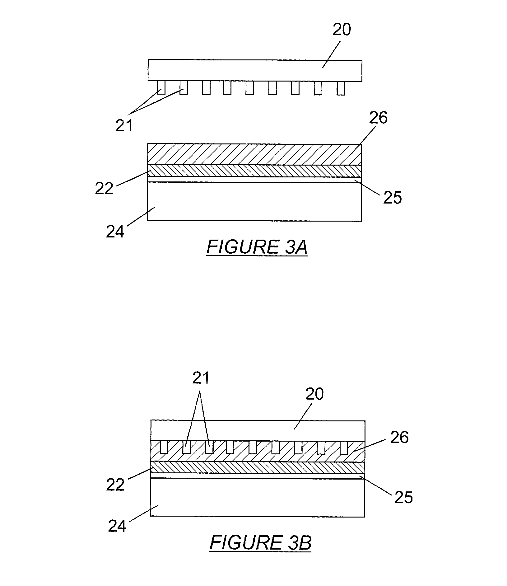
[0031] In this example, aluminum is sputtered on a glass substrate. The thickness of the aluminum film is approximately 590 nm. Diluted PMMA is then spin coated on the aluminum layer on the glass substrate. The thickness of the PMMA is approximately 690 nm. A mold with a grid pattern having a grid period of 570 nm and a depth of 690 nm and the PMMA-coated substrate are heated to 110.degree. C. It takes approximately 3 minutes to stabilize the temperature of the mold and substrate. The mold and PMMA-coated substrate are then compressed together with a pressure of 67 MPa. The mold and the PMMA-coated substrate are maintained at this contacting pressure for 1 minute and then cooled for 4 minutes. After cooling, the mold is removed from the PMMA. A change in the color of the embossed PMMA with changes in viewing angle indicates that the grid pattern has been made on the PMMA. The embossed PMMA and the underlying aluminum layer are dry-etched by BCl.sub.3 / Cl.sub.2N.sub.2 gas flow for 120...

example 3

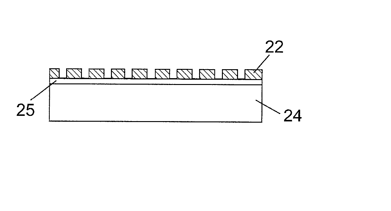
[0039] This example assumes that the bottom layer 44 is made of aluminum, the middle layer 48 is made of silica, and the top layer 46 is made of gold. The grid dimensions are as follows: thickness of the bottom aluminum layer 44 is 466 mn, thickness of the top gold layer 46 is 47 nm, thickness of the middle silica layer 48 is 527 nm, and width of the each grid element 52 is 210 nm. The aspect ratio is 5, the grid period is 396 nm, and the duty cycle is 0.53. The transmission is 85.2% and the contrast ratio is 52.4 dB.

example 4

[0040] This example assumes that the bottom layer 44 is made of gold, the middle layer 48 is made of silicon, and the top layer 46 is made of aluminum. The grid dimensions are as follows: thickness of the bottom gold layer 44 is 412 mn, thickness of the top aluminum layer 46 is 16 mn, thickness of the middle silicon layer 48 is 211 nm, and width of each grid element 52 is 147 nm. The aspect ratio is 4.3, the grid period is 334 nm, and the duty cycle is 0.44. The transmission is 90.9% and the contrast ratio is 40.2 dB.


PUM

PropertyMeasurementUnit
widthaaaaaaaaaa
thicknessaaaaaaaaaa
thicknessaaaaaaaaaa

Abstract

A method for fabricating an integrated optical isolator includes depositing a wire grid material on a magneto-optical substrate and depositing a resist film on the wire grid material. The method further includes bringing a mold with a wire grid pattern on contact with the resist film and compressing the mold and resist film together so as to emboss the wire grid pattern in the resist film. The method further includes transferring the wire grid pattern in the resist film to the wire grid material on the magneto-optical substrate by etching.

Description

BACKGROUND OF INVENTION[0001] 1. Field of the Invention[0002] The invention relates to methods for fabricating integrated optical isolators. More specifically, the invention relates to a method for forming a wire grid polarizer on a Faraday rotator and a method for suppressing reflection of rejected polarization.[0003] 2. Background Art[0004] Fiber-optic communications systems have three major components. These include (1) a transmitter that converts electronic data signals to light signals, (2) an optical fiber that guides the light signals, and (3) a receiver that captures the light signals at the other end of the fiber and converts them to electrical signals. For high-speed data transmission or long-distance applications, the light source in the transmitter is usually a semiconductor laser diode. The transmitter pulses the output of the laser diode in accordance with the data signal to be transmitted and sends the pulsed light into the fiber. In fiber-optic communications systems...

Claims


Application Information

Patent Timeline
Patent Type & Authority Applications(United States)
IPC IPC(8): G02B6/26
CPCG02B6/2746
Inventor BORRELLI, NICHOLAS F.GROSSMAN, DAVID G.HASUI, KENJROKOSAKA, TAMIOVISOVSKY, NICK J.
Owner CORNING INC
Why Eureka
Try Eureka