Zinc blende type CrSb compound, method for fabricating the same, and multilayered structure
- Summary
- Abstract
- Description
- Claims
- Application Information
AI Technical Summary
Benefits of technology
Problems solved by technology
Method used
Image
Examples
example 1
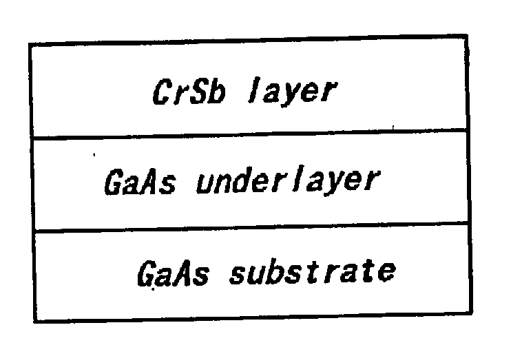
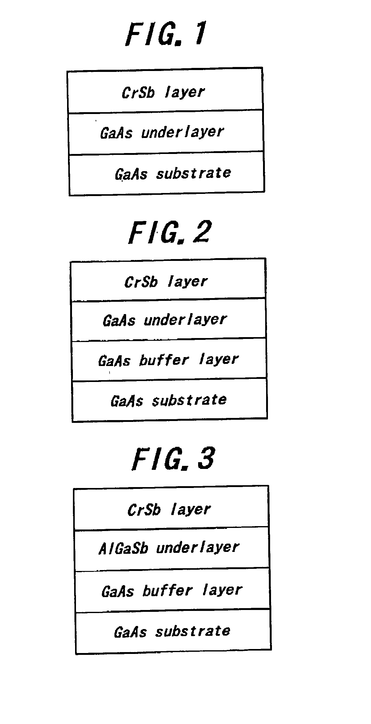
[0034] In this Example, a multilayered structure including a zinc blende type CrSb compound shown in FIG. 1 was fabricated. A (001) GaAs substrate was employed and set in a MBE apparatus. Then, the GaAs substrate was heated to 580.degree. C., and an oxide film was desorbed from the GaAs substrate surface. Then, the GaAs substrate was heated to 560.degree. C., and Ga beams and Sb beams were irradiated simultaneously onto the GaAs substrate, to form a GaAs layer as an underlayer in a thickness of 500 nm on the GaAs substrate.
[0035] Then, the GaAs substrate was cooled down while the Sb beams were irradiated. The irradiation of the Sb beams was stopped when the GaAs substrate was cooled down to 400.degree. C. Then, Cr beams and Sb beams were irradiated simultaneously onto the GaAs underlayer, to form a CrSb layer in a thickness of 0.6 nm on the GaAs underlayer while the GaAs substrate was held at 250.degree. C.
[0036] In this case, the forming rate of the CrSb layer was set to 6 nm / sec. ...
example 2
[0037] In this Example, a multilayered structure including a zinc blende type CrSb compound shown in FIG. 2 was fabricated. A (001) GaAs substrate was employed and set in a MBE apparatus, as mentioned in Example 1. Then, an oxide film was desorbed from the GaAs substrate surface in the same manner. Then, the GaAs substrate was heated to 530.degree. C., and a GaAs buffer layer was formed in a thickness of 100 nm on the GaAs substrate by means of a MBE method. Then, Ga beams and Sb beams were irradiated simultaneously onto the GaAs buffer layer, to form a GaSb underlayer in a thickness of 400 nm on the GaAs buffer layer.
[0038] Then, a CrSb layer was formed in a thickness of 0.6 nm on the GaSb underlayer in the same manner as in Example 1. When the crystallinity of the CrSb layer was investigated by means of reflection high-energy electron diffraction (RHEED), it was turned out that the CrSb layer has zinc blende type RHEED pattern.
example 3
[0039] In this Example, a multilayered structure including a zinc blende type CrSb compound shown in FIG. 3 was fabricated. A (001) GaAs substrate was employed and set in a MBE apparatus, as mentioned in Example 1. Then, an oxide film was desorbed from the GaAs substrate surface in the same manner. Then, the GaAs substrate was heated to 530.degree. C., and a GaAs buffer layer was formed in a thickness of 100 nm on the GaAs substrate by means of a MBE method. Then, Al beams, Ga beams and Sb beams were irradiated simultaneously onto the GaAs buffer layer, to form an AlGaSb underlayer in a thickness of 400 nm on the GaAs buffer layer.
[0040] Then, a CrSb layer was formed in a thickness of 0.3 nm on the AlGaSb underlayer in the same manner as in Example 1. When the crystallinity of the CrSb layer was investigated by means of reflection high-energy electron diffraction (RHEED), it was turned out that the CrSb layer has zinc blende type RHEED pattern.
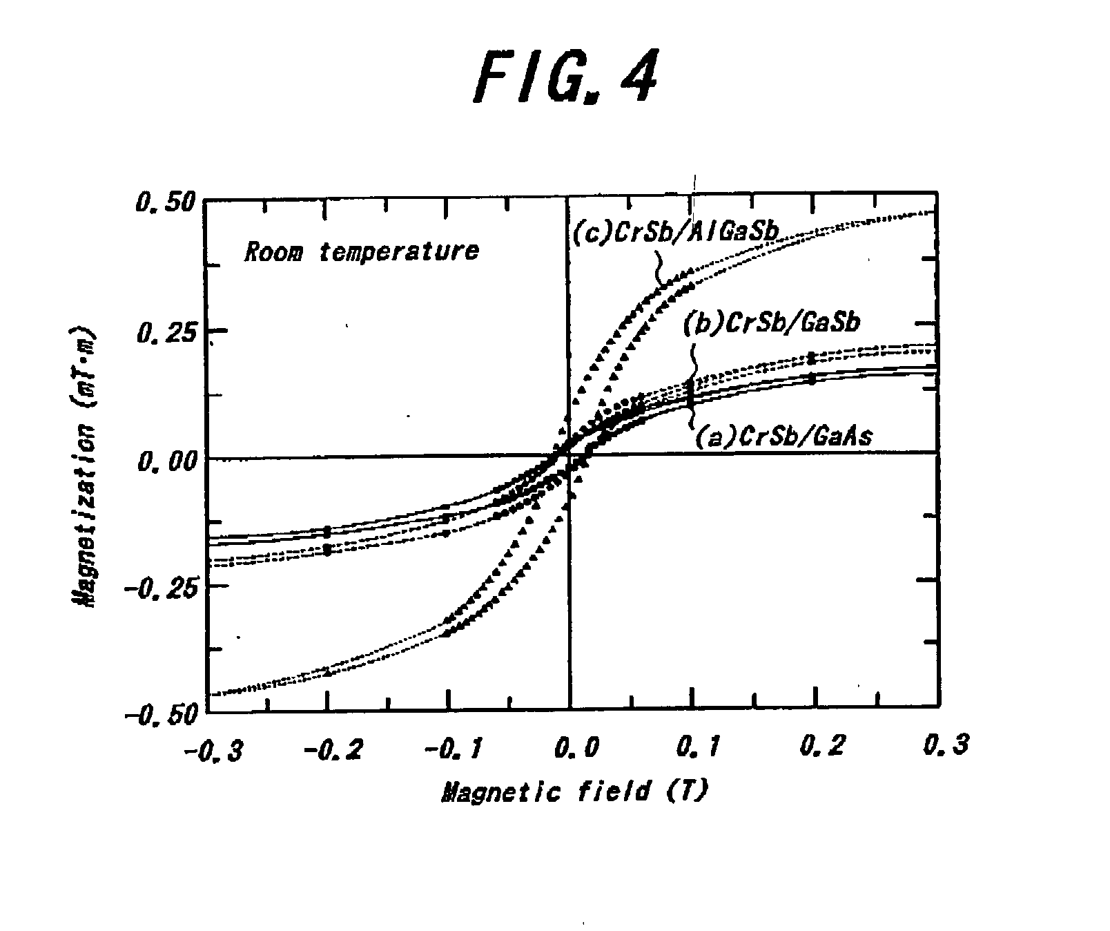
[0041] FIG. 4 shows the magnetization h...
PUM
 Abstract
Description
Claims
Application Information


