Structure and method for fabricating semiconductor structures and devices utilizing the formation of a compliant III-V arsenide nitride substrate used to form the same

a technology of arsenide nitride and semiconductor structure, which is applied in the direction of semiconductor lasers, crystal growth processes, and chemically reactive gases, can solve the problem of low crystalline quality of monocrystalline materials

Inactive Publication Date: 2003-01-16
MOTOROLA INC
View PDF0 Cites 38 Cited by
  • Summary
  • Abstract
  • Description
  • Claims
  • Application Information

AI Technical Summary

Problems solved by technology

These attempts have generally been unsuccessful because lattice mismatches between the host crystal and ...

Method used


Image

  • Structure and method for fabricating semiconductor structures and devices utilizing the formation of a compliant III-V arsenide nitride substrate used to form the same
  • Structure and method for fabricating semiconductor structures and devices utilizing the formation of a compliant III-V arsenide nitride substrate used to form the same
  • Structure and method for fabricating semiconductor structures and devices utilizing the formation of a compliant III-V arsenide nitride substrate used to form the same

Examples


example 2

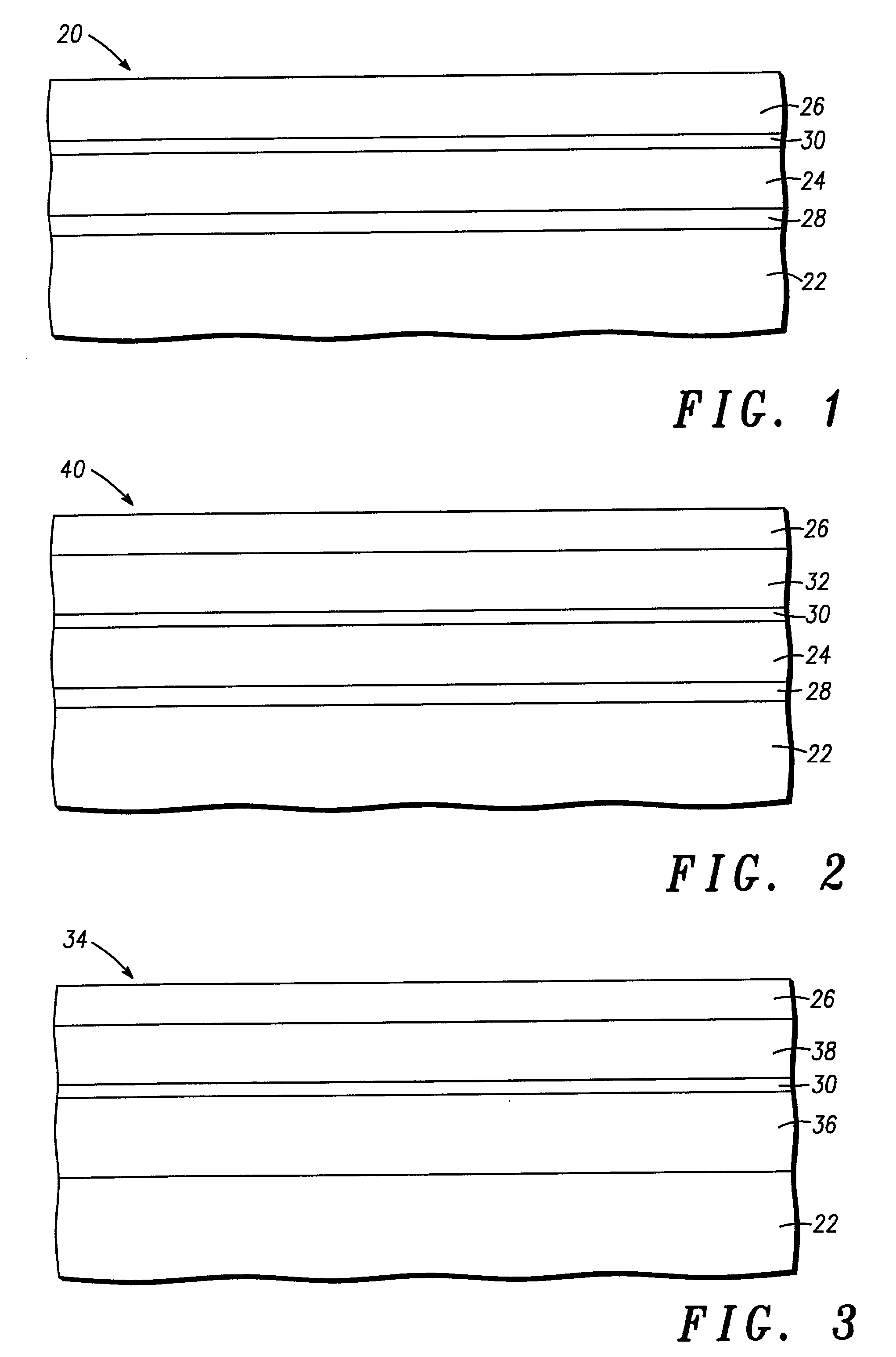
[0040] This example provides exemplary materials useful in structure 34, as illustrated in FIG. 3. Substrate material 22, template layer 30, and monocrystalline material layer 26 may be the same as those described above in connection with example 1.

[0041] Amorphous layer 36 is an amorphous oxide layer which is suitably formed of a combination of amorphous intermediate layer materials (e.g., layer 28 materials as described above) and accommodating buffer layer materials (e.g., layer 24 materials as described above). For example, amorphous layer 36 may include a combination of SiO.sub.x and Sr.sub.zBa.sub.1-zTiO.sub.3 (where z ranges from 0 to 1),which combine or mix, at least partially, during an anneal process to form amorphous oxide layer 36.

[0042] The thickness of amorphous layer 36 may vary from application to application and may depend on such factors as desired insulating properties of layer 36, type of monocrystalline material comprising layer 26, and the like. In accordance w...


PUM


Abstract

High quality epitaxial layers of monocrystalline III-V arsenide nitride materials can be grown overlying monocrystalline substrates such as large silicon wafers by forming a compliant substrate for growing the monocrystalline layers. One way to achieve the formation of a compliant substrate includes first growing an accommodating buffer layer on a silicon wafer. The accommodating buffer layer is a layer of monocrystalline oxide spaced apart from the silicon wafer by an amorphous interface layer of silicon oxide. The amorphous interface layer dissipates strain and permits the growth of a high quality monocrystalline oxide accommodating buffer layer. The accommodating buffer layer is lattice matched to both the underlying silicon wafer and the overlying monocrystalline III-V arsenide nitride material layer. Any lattice mismatch between the accommodating buffer layer and the underlying silicon substrate is taken care of by the amorphous interface layer. In addition, an accommodating buffer layer comprising a barium strontium titanium oxide and a monocrystalline III-V arsenide nitride layer, such as GaAsN, having a nitrogen concentration ranging from 1-5% function to further reduce any lattice mismatch between layers.

Description

FIELD OF THE INVENTION[0001] This invention relates generally to semiconductor structures and devices and to a method for their fabrication, and more specifically to semiconductor structures and devices and to the fabrication and use of semiconductor structures, devices, and integrated circuits that include a monocrystalline material layer comprised of a III-V arsenide nitride semiconductor material. More particularly, the invention is directed to the one step formation of a compliant substrate containing a GaAsN material system on a silicon substrate.BACKGROUND OF THE INVENTION[0002] Semiconductor devices often include multiple layers of conductive, insulating, and semiconductive layers. Often, the desirable properties of such layers improve with the crystallinity of the layer. For example, the electron mobility and band gap of semiconductive layers improves as the crystallinity of the layer increases. Similarly, the free electron concentration of conductive layers and the electron...

Claims


Application Information

Patent Timeline
IPC IPC(8): C30B25/18H01L21/20H01L33/00H01L33/12H01S5/02H01S5/323
CPCC30B25/18H01L21/02381H01L21/02488H01L21/02505H01L21/02513H01L21/0254H01L21/02546H01L33/007H01L33/12H01S5/021H01S5/0218H01S5/32366H01S2301/173
Inventor RAMDANI, JAMALHILT, LYNDEE L.
Owner MOTOROLA INC
Why Eureka
Try Eureka