Semiconductor gallium arsenide compatible epitaxial ferroelectric devices for microwave tunable application

a gallium arsenide and ferroelectric device technology, applied in semiconductor devices, electrical devices, capacitors, etc., can solve the problems of limited work on titanate, difficult epitaxial growth of these oxides on gaas, and high substrate cost, and achieve low dielectric loss, good temperature stability, and high dielectric constant

Active Publication Date: 2015-02-26
THE HONG KONG POLYTECHNIC UNIV
View PDF0 Cites 9 Cited by
  • Summary
  • Abstract
  • Description
  • Claims
  • Application Information

AI Technical Summary

Benefits of technology

[0008]Accordingly, the first aspect of the presently claimed invention is to provide a barium strontium titanate / strontium titanate / gallium arsenide heterostructure for tunable ferroelectric devices. The heterostructure of the present invention comprises a gallium arsenide (GaAs) substrate, at least one layer of strontium titanate, SrTiO3 (STO), which is grown on a surface of the gallium arsenide substrate, and at least one layer of barium strontium titanate, Ba1-xSrxTiO3 (BST), which is grown on top of the layer of STO in order to form an epitaxial BST / STO / GaAs heterostructure useful in fabrication of tunable ferroelectric devices. The highly epitaxial BST / STO / GaAs heterostructure of the present invention has many advantages including good temperature stability, high dielectric constant and low dielectric loss, which are important factors for fabricating tunable ferroelectric devices.

Problems solved by technology

However, the problems are the high cost of the substrates and the fact that oxide substrates of MgO and LAO are only available in small geometries, which are not suitable for mass production.
Additionally, the use of oxide substrates, preferably, requires mounting complicated hybrid microwave integrated circuits.
Compared to the growth of perovskite titanates on Si, there is limited work on the titanate oxide / III-V's heteroepitaxial structures while many properties and functionalities of such heterostructures are expected.
Nevertheless, the thin films deposited by these techniques are usually amorphous and polycrystalline which have a lot of defects and are hardly applied in the semiconductor devices.
The epitaxial growth of these oxides on GaAs is rather challenging, since GaAs is neither chemically stable nor thermally stable.
To date, there is no work on the tunable microwave device application using epitaxial ferroelectric thin films grown on GaAs.
So far, no similar products integrating ferroelectric devices with GaAs exist in the market.

Method used


Image

  • Semiconductor gallium arsenide compatible epitaxial ferroelectric devices for microwave tunable application
  • Semiconductor gallium arsenide compatible epitaxial ferroelectric devices for microwave tunable application
  • Semiconductor gallium arsenide compatible epitaxial ferroelectric devices for microwave tunable application

Examples


Embodiment Construction

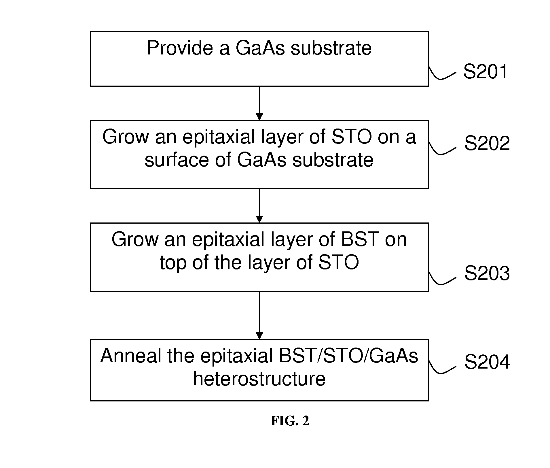
[0024]In the following description, several BST / STO / GaAs heterostructures and methods for fabricating the BST / STO / GaAs heterostructure thereof are set forth as preferred examples. It will be apparent to those skilled in the art that modifications, including additions and / or substitutions maybe made without departing from the scope and spirit of the invention. Specific details may be omitted so as not to obscure the invention; however, the disclosure is written to enable one skilled in the art to practice the teachings herein without undue experimentation.

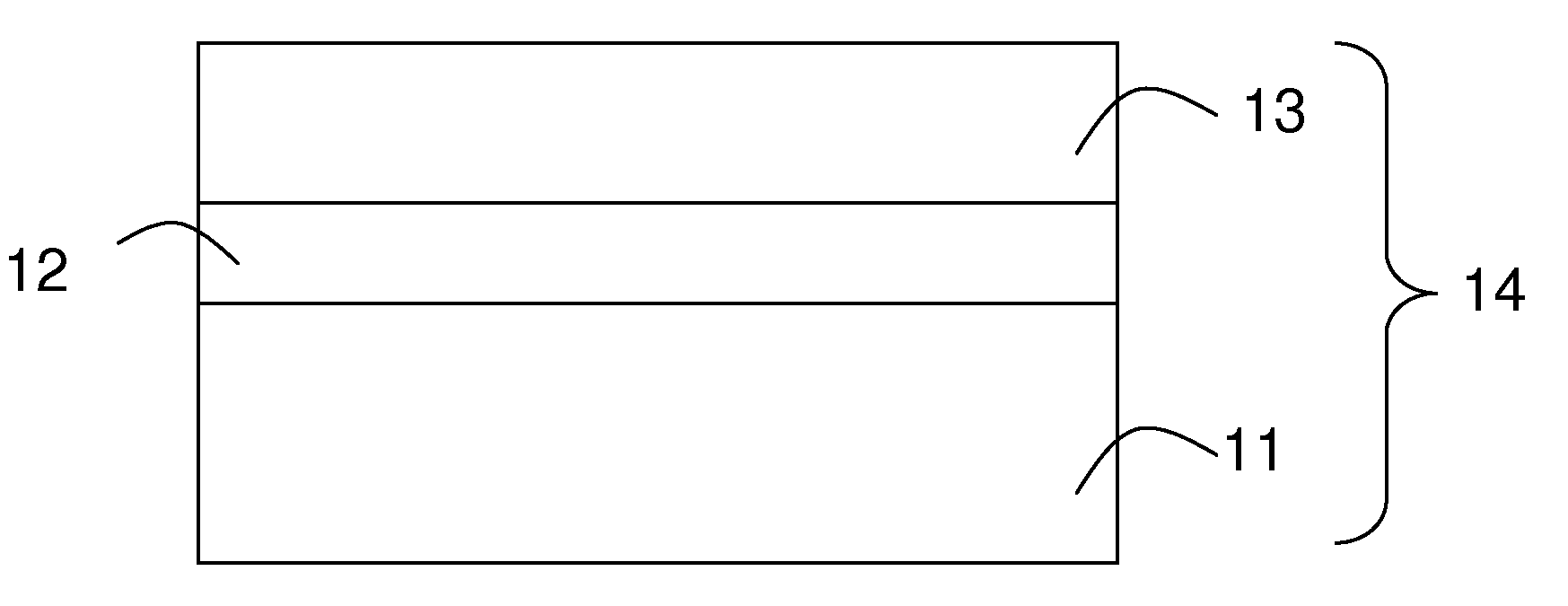
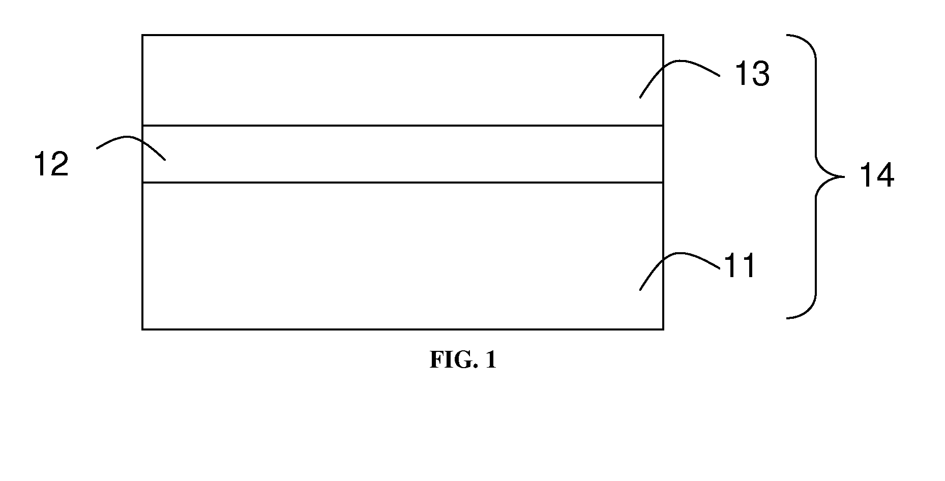
[0025]FIG. 1 shows a BST / STO / GaAs heterostructure according to one embodiment of the presently claimed invention. The BST / STO / GaAs heterostructure of the present invention comprises a GaAs substrate 11, a layer of strontium titanate (STO) 12 grown on a surface of the GaAs substrate 11, and a layer of barium strontium titanate (BST) 13 grown on top of the layer of STO 12 in order to form an epitaxial BST / STO / GaAs heterostructure 14.

[...


PUM

PropertyMeasurementUnit
operation wavelengthaaaaaaaaaa
temperatureaaaaaaaaaa

Abstract

The presently claimed invention provides a barium strontium titanate / strontium titanate / gallium arsenide (BST / STO / GaAs) heterostructure comprising a gallium arsenide (GaAs) substrate, at least one strontium titanate (STO) layer, and at least one barium strontium titanate (BST) layer. The BST / STO / GaAs heterostructure of the present invention has a good temperature stability, high dielectric constant and low dielectric loss, which enable to fabricate tunable ferroelectric devices. A method for fabricating the BST / STO / GaAs heterostructure is also disclosed in the present invention, which comprises formation of at least one STO layer on the GaAs substrate by a first laser molecular beam epitaxial system, and formation of at least one BST layer on the STO layer by a second laser molecular beam epitaxial system.

Description

COPYRIGHT NOTICE[0001]A portion of the disclosure of this patent document contains material, which is subject to copyright protection. The copyright owner has no objection to the facsimile reproduction by anyone of the patent document or the patent disclosure, as it appears in the Patent and Trademark Office patent file or records, but otherwise reserves all copyright rights whatsoever.FIELD OF THE INVENTION[0002]The present invention relates generally to a highly epitaxial barium strontium titanate / strontium titanate / gallium arsenide (BST / STO / GaAs) heterostructure, and a method for fabricating the epitaxial heterostructure, and more specifically, the present invention relates to a BST / STO / GaAs heterostructure, which is used for tunable ferroelectric devices.TECHNICAL BACKGROUND[0003]Ferroelectric oxides are very attractive materials with unique chemical and physical properties, which can be used for a variety of devices. Among these devices, frequency and phase agile microwave devi...

Claims


Application Information

Patent Timeline
Patent Type & Authority Applications(United States)
IPC IPC(8): H01L21/02H01L29/205
CPCH01L29/205H01L21/02631H01G7/06H01L29/452H01L29/93H01L28/60H01L28/88
Inventor HAO, JIANHUAHUANG, WENYANG, ZHIBIN
Owner THE HONG KONG POLYTECHNIC UNIV
Why Eureka
Try Eureka