

Method for transferring element, method for producing element, integrated circuit, circuit board, electro-optical device, IC card, and electronic appliance
a technology of element and method, applied in the direction of transportation and packaging, chemistry apparatus and processes, printing, etc., can solve the problems of lowering the heat resistance (reliability) of semiconductor application devices, el elements and plastic substrates are susceptible to such elevated temperatures, ablation and peeling,
- Summary
- Abstract
- Description
- Claims
- Application Information
AI Technical Summary
Benefits of technology
Problems solved by technology
Method used
Image

Examples
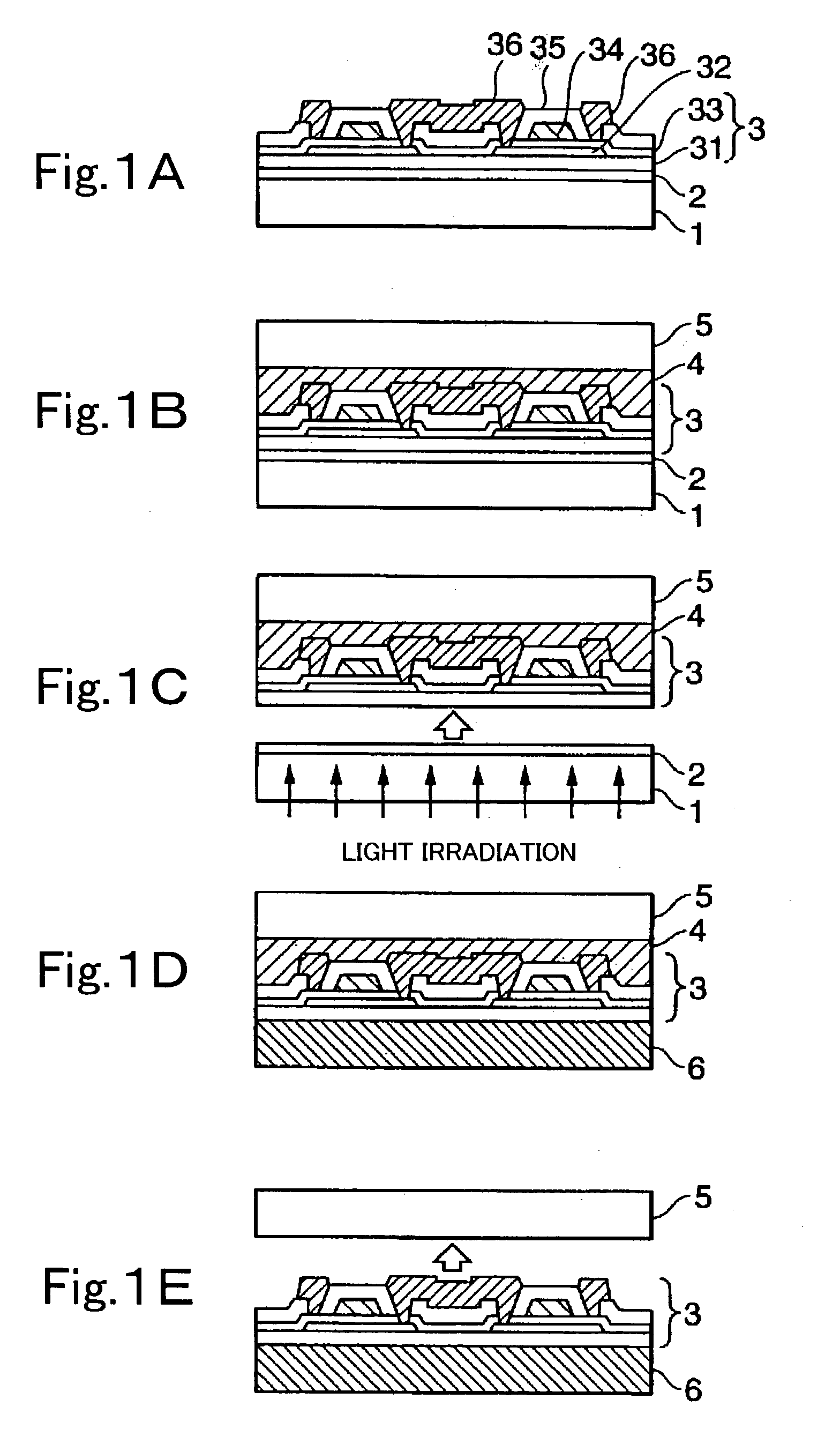
first embodiment
[0118] That is, the present invention results in a thinner semiconductor device because it has no adhesive layer between the transfer substrate and element-forming layer such as in conventional devices. The material for the resin substrate serving as the underlayer substrate of the element-forming layer may be selected upon a consideration of the adhesion with the element-forming layer and the like, a wide range of materials may be selected, and it is easier to ensure that the thermal expansion properties are closer together. Final products with matching conditions such as the coefficient of thermal expansion are less susceptible to cracking and warping due to heat, and have better heat resistance.
[0119] Particularly in cases where a large substrate area is required, such as when the final product is a large-scale display device, a thin resin substrate can be used for the final product while the invention in this embodiment is used to manufacture a pixel circuit for an active matrix...
second embodiment
[0121] Second Embodiment
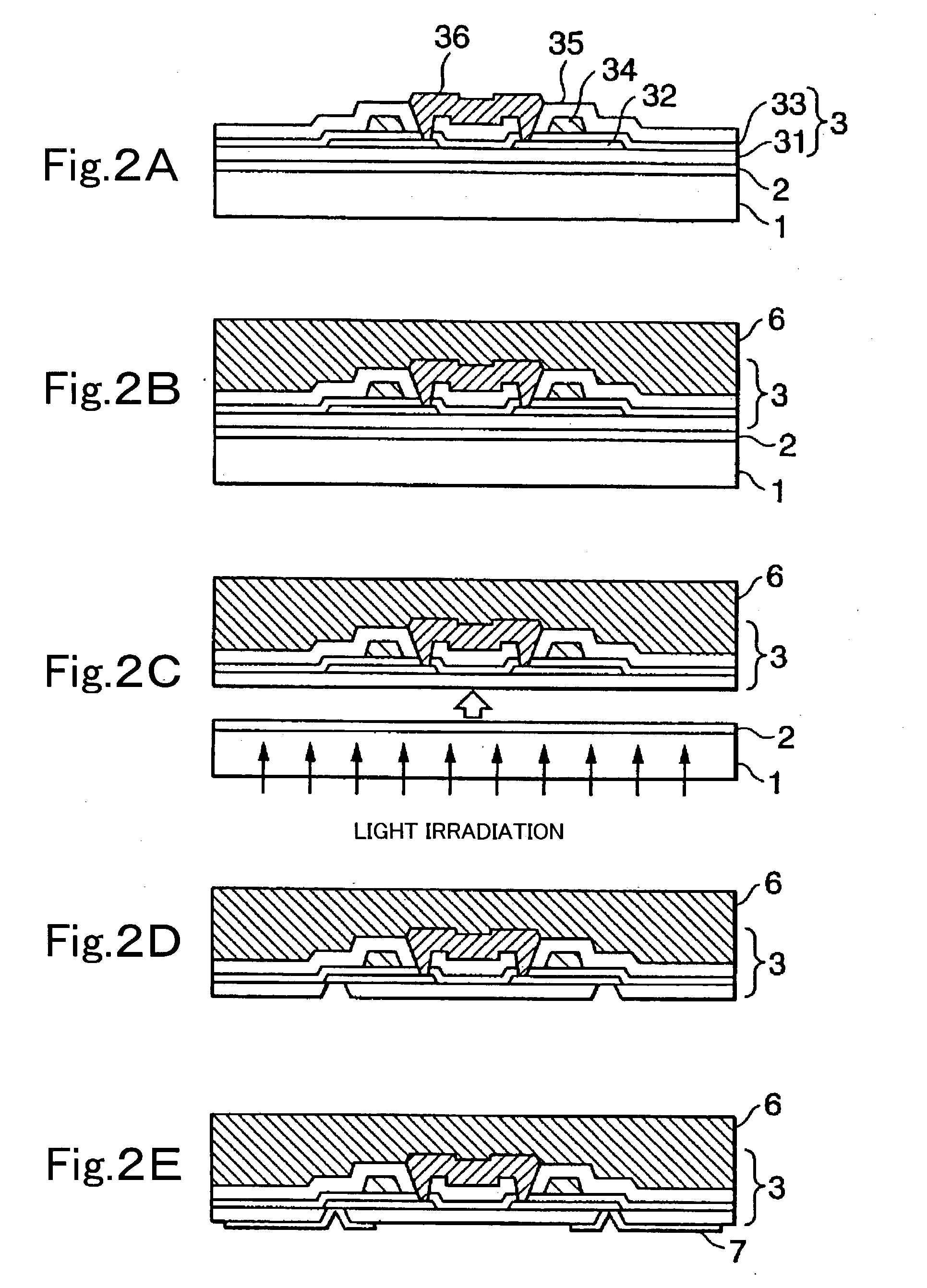
[0122] The second embodiment of the present invention relates to a second method of transfer in which resin is applied onto the element-forming layer and cured to form a transfer substrate, and the original substrate is removed. More particularly, this is a method of transfer in which there is no need for laminating a previous transfer substrate.
[0123] FIGS. 2A through 2E illustrate the process (steps) for producing an element and circuit board in the second embodiment of the invention. Parts that are the same as those in the first embodiment are indicated by the same symbols. In this second embodiment, the use of temporary transfer substrate 5 is omitted and, therefore, the transfer is conducted once.
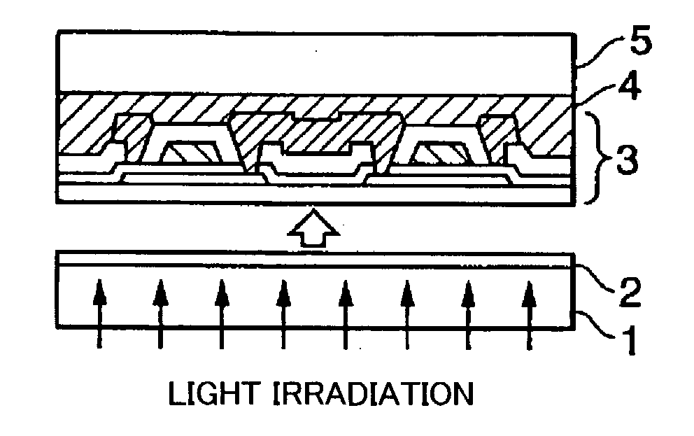
[0124] First, as illustrated in FIG. 2A, a peeling layer 2 is formed on a heat-resistant element-forming substrate 1 such as quartz glass. As described above, the peeling layer 2 has the property of separation through internal separation when exposed to heat, li...
third embodiment
[0134] Third Embodiment
[0135] The third embodiment is an integrated circuit produced by the methods of transfer in the aforementioned embodiments, and is a circuit board.
[0136] The integrated circuit in this embodiment relates to a static RAM which is an LSI formed by the method for transferring an element in the present invention. FIG. 4A is a plan of the integrated circuit of this embodiment, FIG. 4B is a partial cross sectional detail of line A-A in FIG. 4A featuring the use of the first embodiment, and FIG. 4C is a partial cross sectional detail of the use of the second embodiment.
[0137] As illustrated in FIG. 4A, the integrated circuit 100 comprises individual blocks of a memory array 101, address buffer 102, row decoder 103, word driver 104, address buffer 105, column decoder 106, column selector switch 107, input / output circuit 108, and control circuit 109. Thin-film transistor-based circuits are formed in each block, and wiring comprising patterned metal layers is formed bet...
PUM
| Property | Measurement | Unit |
|---|---|---|
| Force | aaaaa | aaaaa |
| Flexibility | aaaaa | aaaaa |
| Impact resistance | aaaaa | aaaaa |
Abstract
Description
Claims
Application Information