Method for manufacturing semiconductor device, adhesive sheet for use therein and semiconductor device

Inactive Publication Date: 2005-02-22
NITTO DENKO CORP
View PDF7 Cites 12 Cited by
  • Summary
  • Abstract
  • Description
  • Claims
  • Application Information

AI Technical Summary

Benefits of technology

In the step (2) of the manufacturing method according to this invention, the semiconductor element is attached to the adhesive layer of the adhesive sheet, which serves as a supporting member. In the step (5) of the manufacturing method, the adhesive sheet is detached from the formed semiconductor device. The manufacturing method of this invention is free from the metal (die pad) and the adhesive layer that have been additionally incorporated into the conventional process to fix the semiconductor element. Therefore, the method of this invention can produce a thinner semiconductor device.
The semiconductor element attached to the adhesive sheet is prevented from shifting in the transfer step and the like. In the step (4) such as the step of transfer-molding a sealing resin, the s

Problems solved by technology

Thus, the packages with the lead frame have been relatively large in size and relatively thick.
Such a structure may still have a problem in satisfying the demand for small thin semiconductor devices in the industrial field.
However, the material of the base member 3 such as a fluoropolymer, silicone, and a fluoro-coated metal as disclosed in the publication can never satisfy the above contrary requirements for the contact.
Such a structure may stil

Method used


Image

  • Method for manufacturing semiconductor device, adhesive sheet for use therein and semiconductor device
  • Method for manufacturing semiconductor device, adhesive sheet for use therein and semiconductor device
  • Method for manufacturing semiconductor device, adhesive sheet for use therein and semiconductor device

Examples


example 1

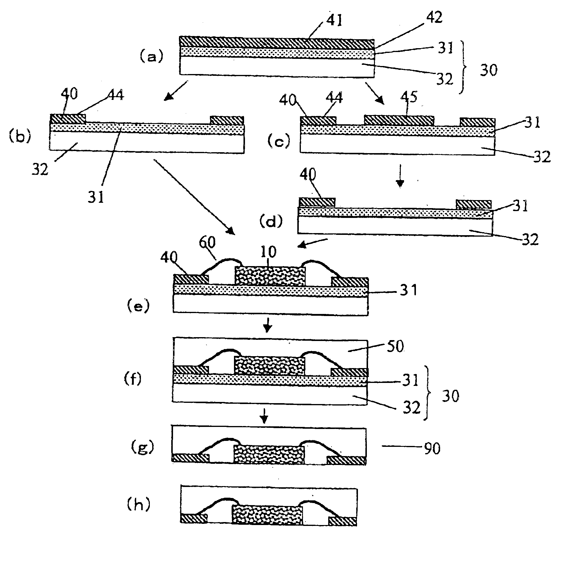
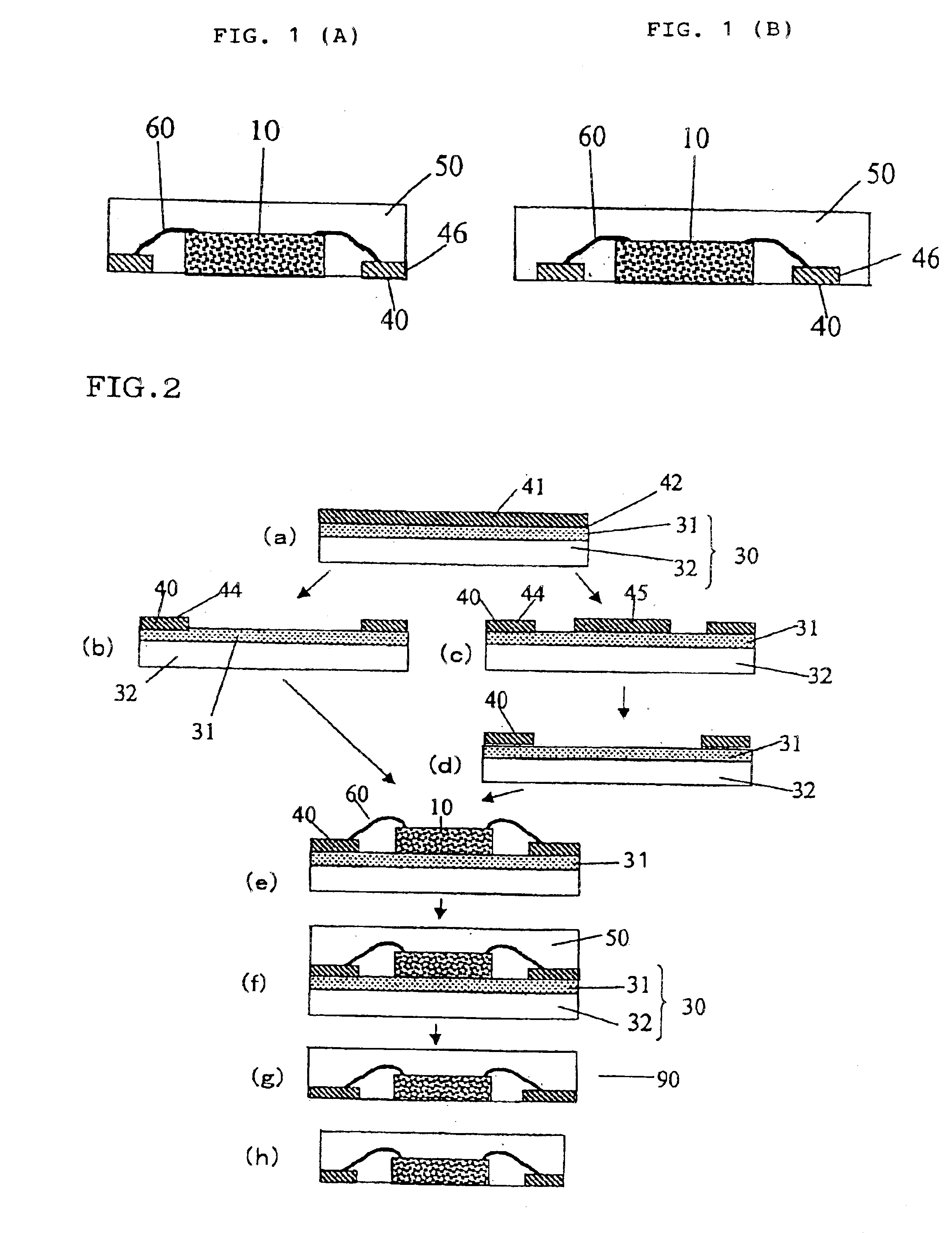
Production of Adhesive Sheet

A silicone-based adhesive (SD-4587L, Toray Dow Corning Co., Ltd.) was applied onto a polyimide film with a thickness of 25 μm and a width of 500 mm (Kapton®H, Du Pont-Toray Co., Ltd.) and then dried at 150° C. for 3 minutes to form an adhesive sheet having an adhesive layer with a thickness of 5 μm. The adhesive layer of the adhesive sheet had an elastic modulus of 0.15 MPa at 150° C. and an adhesive strength of 0.25 N / 10 mm to a silicon mirror wafer. The polyimide film used as the base layer had an elastic modulus of 1.8 GPa at 150° C.

Fabrication of Semiconductor Device

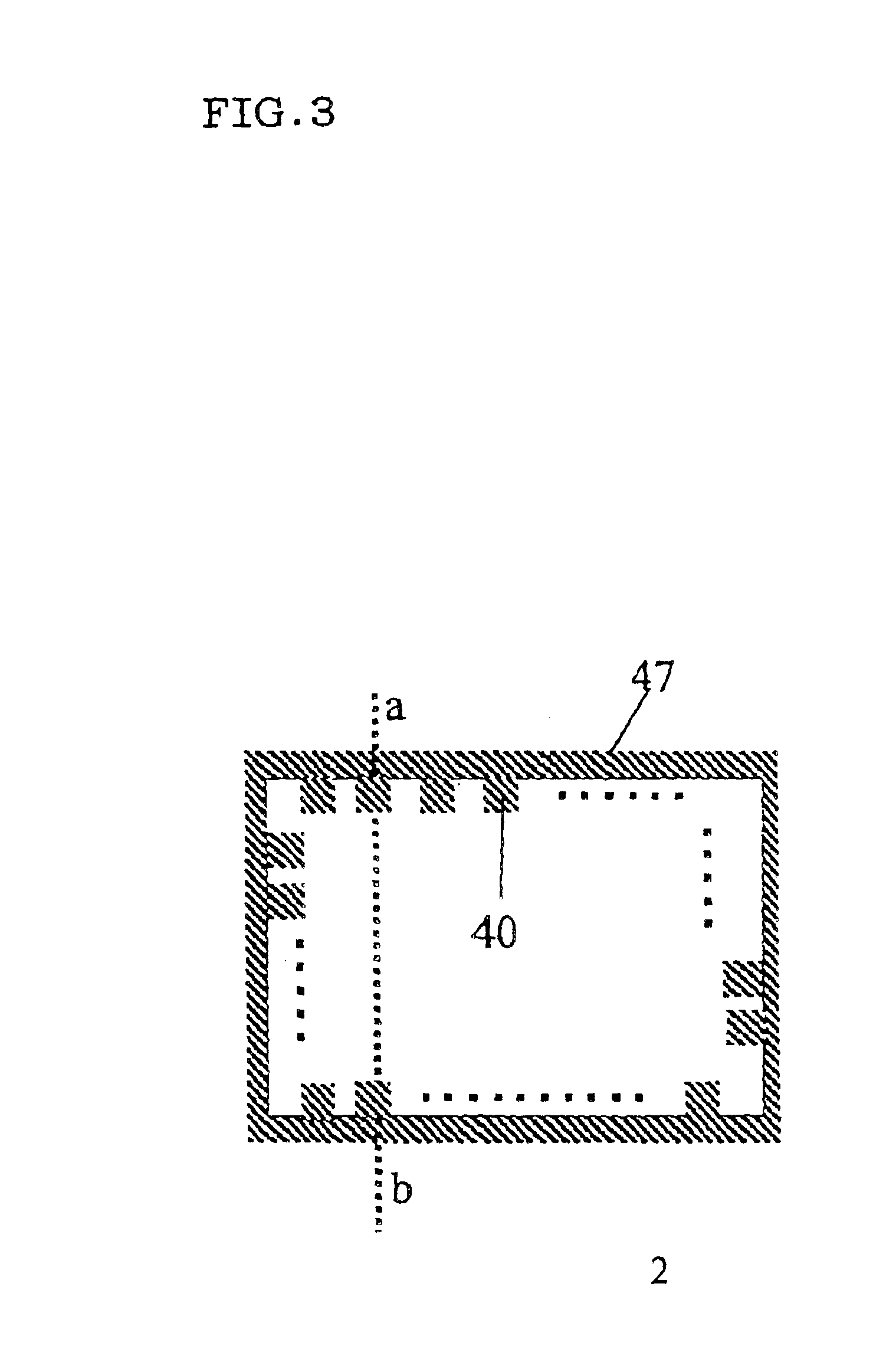
A copper metal foil with a thickness of 35 μm (BHY-138T, Japan Energy Corporation) was attached to the adhesive layer of the adhesive sheet to form a flexible metal-attached adhesive sheet. After pattern etching, one block corresponding to each block 80 (with a W1 of 500 mm) as shown in FIG. 5 had an arrangement of the electrically conductive parts 40 as shown in FIG. 7. Referring to FIG. ...

example 2

The process of Example 1 was used to form semiconductor devices except that the metal foil used was a copper-nickel alloy foil with a thickness of 18 μm (C7025, Japan Energy Corporation). The wire bonding had a 100% success rate. The observation of the inside of the resulting semiconductor devices proved that the y had no deformed wire, no shifted chip, or the like.

Wire Bonding Conditions

Apparatus: UTC-300BI SUPER (Shinkawa Ltd.)Ultrasonic Frequency: 115 kHzUltrasonic Output Time: 15 millisecondsUltrasonic Output Power: 120 mWBond Load: 1.18 NSearch Load: 1.37 N

Transfer Molding ConditionsApparatus: TOWA Molding MachineMolding Temperature: 175° C.Time: 90 secondsClamp Pressure: 200 kNTransfer Speed: 3 mm / secondTransfer Pressure: 5 kN

Elastic Modulus Determining Method

The elastic modulus of the base layer and the adhesive layer were measured under the following conditions:Evaluation System: Rheometrics Viscoelastic Spectrometer (ARES)Temperature Rise Rate: 5° C. / minFrequency: 1 HzMeasu...


PUM


Abstract

A method for manufacturing a semiconductor device includes the steps of: (1) forming a plurality of electrically conductive parts on portions of an adhesive layer of an adhesive sheet, the adhesive sheet having a base layer and the adhesive layer; (2) attaching at least one semiconductor element having electrodes to the adhesive layer, wherein an electrode-free side of the semiconductor element is attached to the adhesive layer; (3) electrically connecting a wire between each of the electrically conductive parts and each of the electrodes of the semiconductor element; (4) sealing the semiconductor element in a sealing resin to form a semiconductor device on the adhesive sheet; and (5) separating the adhesive sheet from the semiconductor device. This method enables the production of thin semiconductor devices with a surface mount type.

Description

BACKGROUND OF THE INVENTION1. Field of the InventionThe present invention relates to a method for manufacturing a surface mount type semiconductor device with leadless structure. In particular, this invention relates to a method for manufacturing a thin semiconductor device with low-cost. This invention also relates to an adhesive sheet for use in such a method for manufacturing a semiconductor device. This invention further relates to a surface mount type semiconductor device with leadless structure, which is thin and with low-cost.2. Description of the Related ArtPackages of individual components such as semiconductor integrated circuits, transistors, and diodes have been made smaller and thinner. In the field of semiconductor integrated circuits with lead frames, there has been a demand for a finer lead pitch of the lead frames for the purpose of forming a larger number of pins. If the lead width is reduced to meet such a demand, however, the strength of the lead is reduced so th...

Claims


Application Information

Patent Timeline
IPC IPC(8): H01L21/68H01L21/02H01L23/31H01L23/28H01L21/67H01L21/48H01L23/12H01L21/56
CPCH01L21/4832H01L21/568H01L23/3107H01L24/32H01L2224/85205H01L2224/45015H01L24/45H01L2924/10253H01L2224/45144H01L2924/0133H01L2924/0132H01L2924/01087H01L2924/01074H01L2924/01045H01L2924/01042H01L2924/01024H01L2924/01019H01L2924/01006H01L2924/01005H01L24/48H01L2924/18165H01L2924/01082H01L2924/01079H01L2924/01078H01L2924/01059H01L2924/01051H01L2224/32245H01L2224/48091H01L2224/48247H01L2224/73265H01L2224/85001H01L2924/01013H01L2924/01029H01L2924/01033H01L2924/01047H01L2924/00014H01L2924/01026H01L2924/01028H01L2924/01027H01L2924/3512H01L2924/00H01L2924/20305H01L2924/181H01L2924/14H01L2924/20752H01L2924/00012
Inventor HOSOKAWA, KAZUHITOOKEYUI, TAKUJIFUJII, HIROFUMIYAMAMOTO, YASUHIK
Owner NITTO DENKO CORP
Why Eureka
Try Eureka