Method for manufacturing electroluminescence display panel and evaporation mask

a technology of electroluminescence display panel and evaporation mask, which is applied in the direction of electroluminescent light source, vacuum evaporation coating, coating, etc., can solve the problem of inability to employ a method, inability to achieve sufficient and stricter precision for patterning the organic layer

Inactive Publication Date: 2003-03-06
SANYO ELECTRIC CO LTD
View PDF6 Cites 13 Cited by
  • Summary
  • Abstract
  • Description
  • Claims
  • Application Information

AI Technical Summary

Problems solved by technology

For example, because a material for an organic layer used in a low molecular weight organic EL element is vulnerable to moisture, it is not possible to employ a method, for example, in which an organic layer is first formed on the entire surface of the substrate and then the organic layer is etched and patterned into a predetermined shape.
However, in practice, a problem has been found in that patterning with sufficient precision cannot be achieved when evaporation is performed using a nickel mask.
However, in a high resolution display panel, because the area of each pixel is very small, the requirement of precision for patterning the organic layer is stricter, and thus, pattern mismatch of the organic layer caused by the mask deformation is a crucial problem.
When the area of the evaporation mask is increased, the problem of the position mismatch becomes more significant as thermal deformation occurs in the evaporation mask in addition to the increase in the amount of deformation due to the weight of the evaporation mask itself.

Method used


Image

  • Method for manufacturing electroluminescence display panel and evaporation mask
  • Method for manufacturing electroluminescence display panel and evaporation mask
  • Method for manufacturing electroluminescence display panel and evaporation mask

Examples


Embodiment Construction

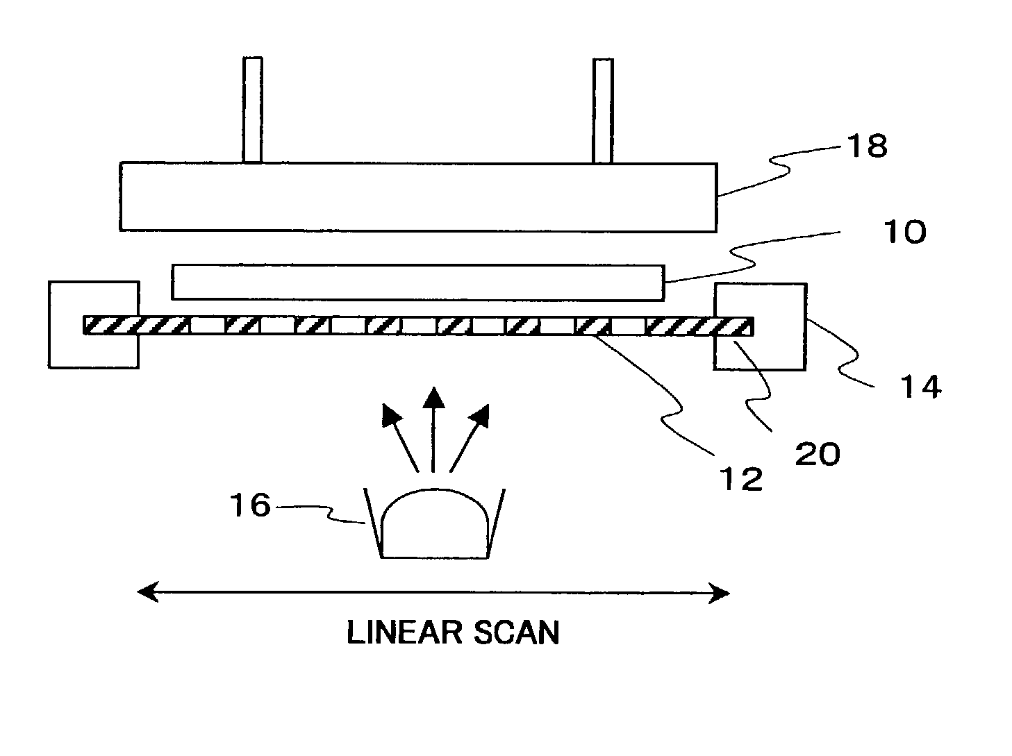
[0025] A preferred embodiment of the present invention (hereinafter simply referred to simply as "the embodiment") will now be described referring to the drawings. FIG. 1 is a diagram for explaining an evaporation process for an organic layer or the like of an organic EL panel according to the embodiment.

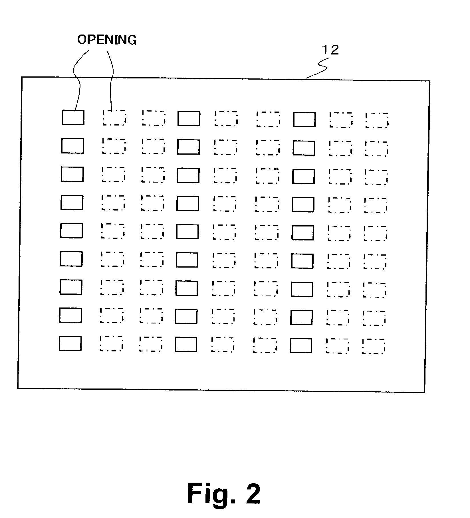
[0026] A glass substrate 10 for an EL panel is placed within an evaporation chamber of a vacuum evaporation device with its surface for evaporation facing downward. An evaporation mask 12 which is larger than the glass substrate 10 is placed below the glass substrate 10. In FIG. 1, the glass substrate 10 and the evaporation mask 12 are shown to be distanced from each other, but, in practice, the glass substrate 10 and the evaporation mask 12 are in contact with each other over almost the entire surface with no gap formed in between. The ends of the evaporation mask 12 are supported by a supporting mechanism 14.

[0027] Below the evaporation mask 12, an evaporation source 16 is placed ...


PUM

PropertyMeasurementUnit
temperatureaaaaaaaaaa

Abstract

An evaporation mask onto which an opening is formed for selectively allowing passage of an evaporation substance from an evaporation source onto a glass substrate to form an evaporation layer of an electroluminescence element in a predetermined pattern is placed between an evaporation source and a glass substrate and evaporation is performed. As a material for the evaporation mask, a material having a thermal expansion coefficient 160% or smaller of the thermal coefficient of glass is employed so as to minimize the thermal deformation of the evaporation mask which is closer the evaporation source and temperature of which is increased, to thereby improve the evaporation patterning precision.

Description

[0001] 1. Field of the Invention[0002] The present invention relates to an evaporation process performed when an electroluminescence (EL) element is formed on a glass substrate.[0003] 2. Description of the Related Art[0004] A type of EL display panel is known in which an organic EL element or the like is employed as an emissive element in each pixel. Expanding use of such an EL display panel as a self-illuminating flat panel is widely expected.[0005] As an organic EL element, a structure is known, for example, in which an anode made of a transparent electrode such as ITO (Indium Tin Oxide) and a cathode made of a metal electrode such as Al or a magnesium alloy are layered on a glass substrate, with an organic layer including an emissive layer provided between the anode and cathode.[0006] For manufacturing such an organic EL element, an evaporation method is employed for forming the organic layer and the metal electrode. During the evaporation, an evaporation mask in which openings a...

Claims


Application Information

Patent Timeline
Patent Type & Authority Applications(United States)
IPC IPC(8): C23C14/04H01L27/32H01L51/40H05B33/10H01L51/56
CPCC23C14/042H01L27/3211H01L27/3244H01L51/001H01L51/56H10K59/35H10K59/12H10K71/164H10K71/00H05B33/10
Inventor NISHIKAWA, RYUJIYAMADA, TSUTOMU
Owner SANYO ELECTRIC CO LTD
Why Eureka
Try Eureka