Amorphous silicon sensor with micro-spring interconnects for achieving high uniformity in integrated light-emitting sources

a micro-spring interconnect and sensor technology, applied in semiconductor lasers, radiation controlled devices, semiconductor/solid-state device details, etc., can solve the problem of high spatial frequency, non-uniform laser response, and the effect of printed images is noticeable to the human ey

Inactive Publication Date: 2003-03-27
XEROX CORP
View PDF4 Cites 37 Cited by
  • Summary
  • Abstract
  • Description
  • Claims
  • Application Information

AI Technical Summary

Problems solved by technology

A drawback of such a large number or light sources, ultra-high density-packed, is the expectation of non-uniformity of laser responses.
This non-uniformity has the potential for high spatial frequency that makes the effect on printed images noticeable to the human eye.
A problem with this process is that it does not address aging of the lasers, fluctuations in driver chip op...

Method used


Image

  • Amorphous silicon sensor with micro-spring interconnects for achieving high uniformity in integrated light-emitting sources
  • Amorphous silicon sensor with micro-spring interconnects for achieving high uniformity in integrated light-emitting sources
  • Amorphous silicon sensor with micro-spring interconnects for achieving high uniformity in integrated light-emitting sources

Examples


second embodiment

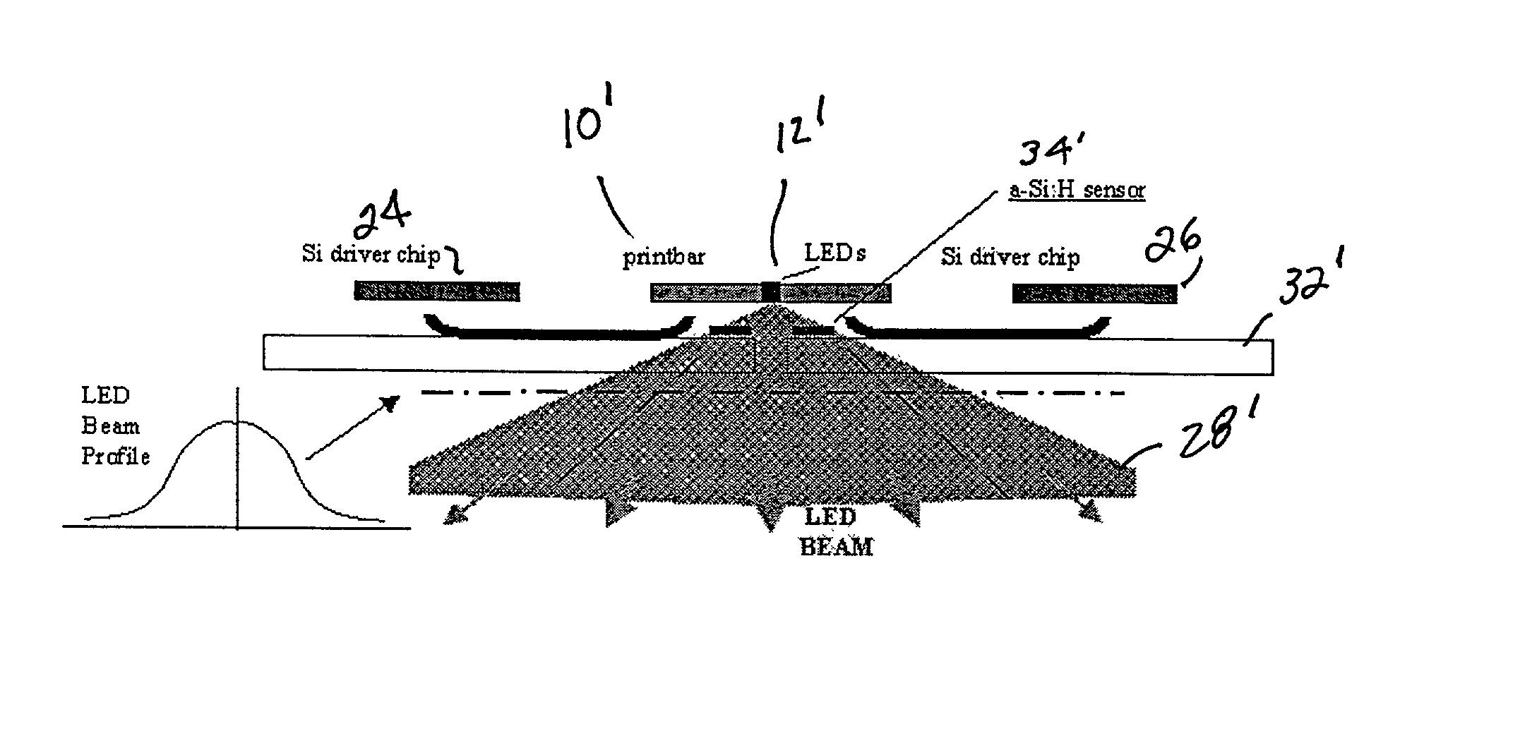
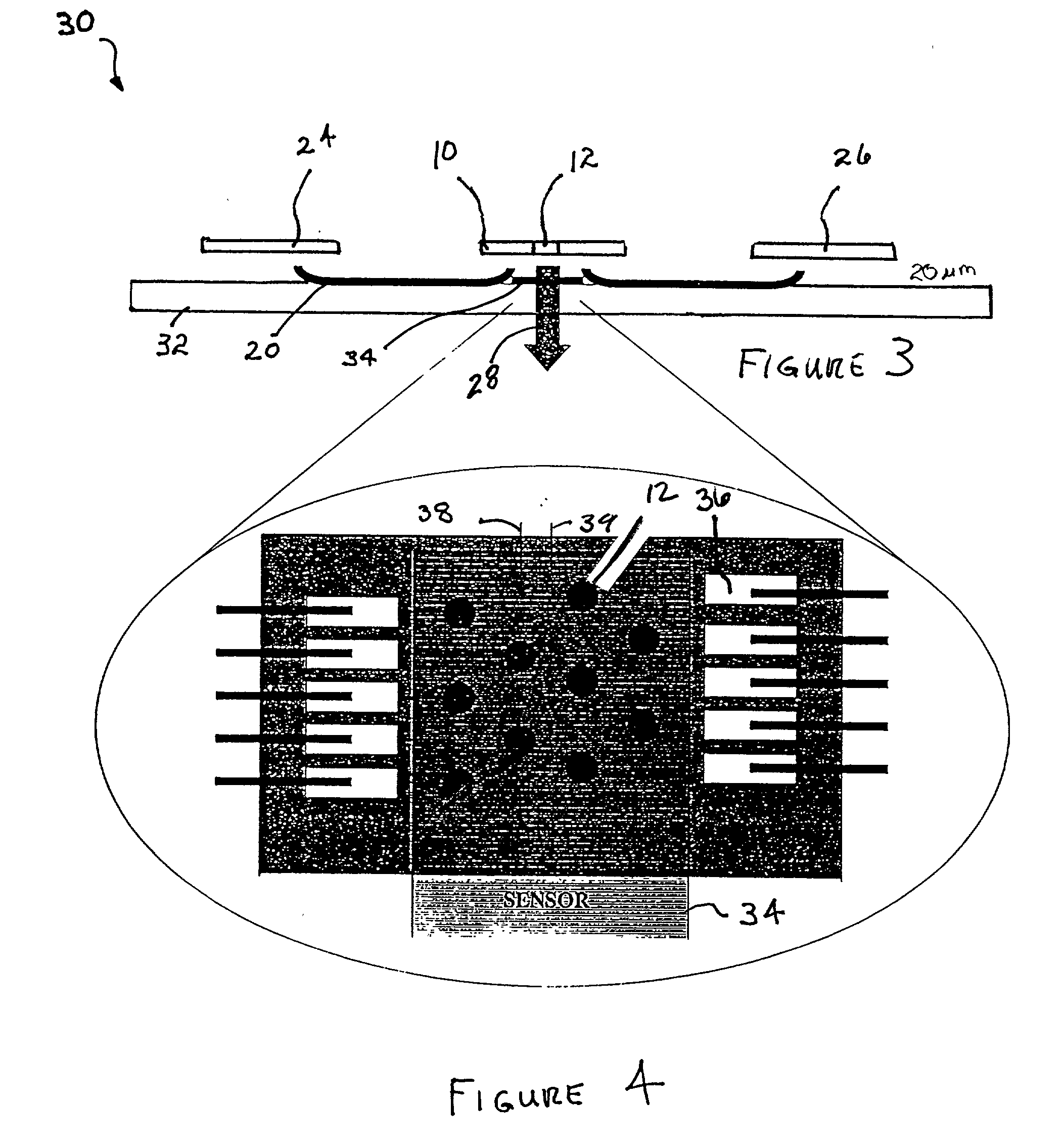
[0065] Turning to FIGS. 7a-b and 8a-b, the present invention is illustrated. It is known that prior to a laser starting its lasing process a phenomenon takes place known as spontaneous emissions. During the spontaneous emissions, light in the visible range from the laser may be emitted. It is undesirable to have this light, as well as light of any other undesired wavelength, reaching sensor element 44. Therefore, to further improve the reliability of the present invention, when IR lasers are used, an additional processing step may be added. Particularly, after the application of second transparent / conductive layer 46 (as depicted in FIG. 5b), a visible light absorption layer 64, which may be hydrogenated amorphous silicon (a-Si:H), is deposited on top of second transparent / conductive layer 46 prior to sensor element 44 and second transparent / conductive layer 46 being patterned. Visible light absorption layer 64 is opaque to visible light, and transparent to IR light. Once sensor ele...

first embodiment

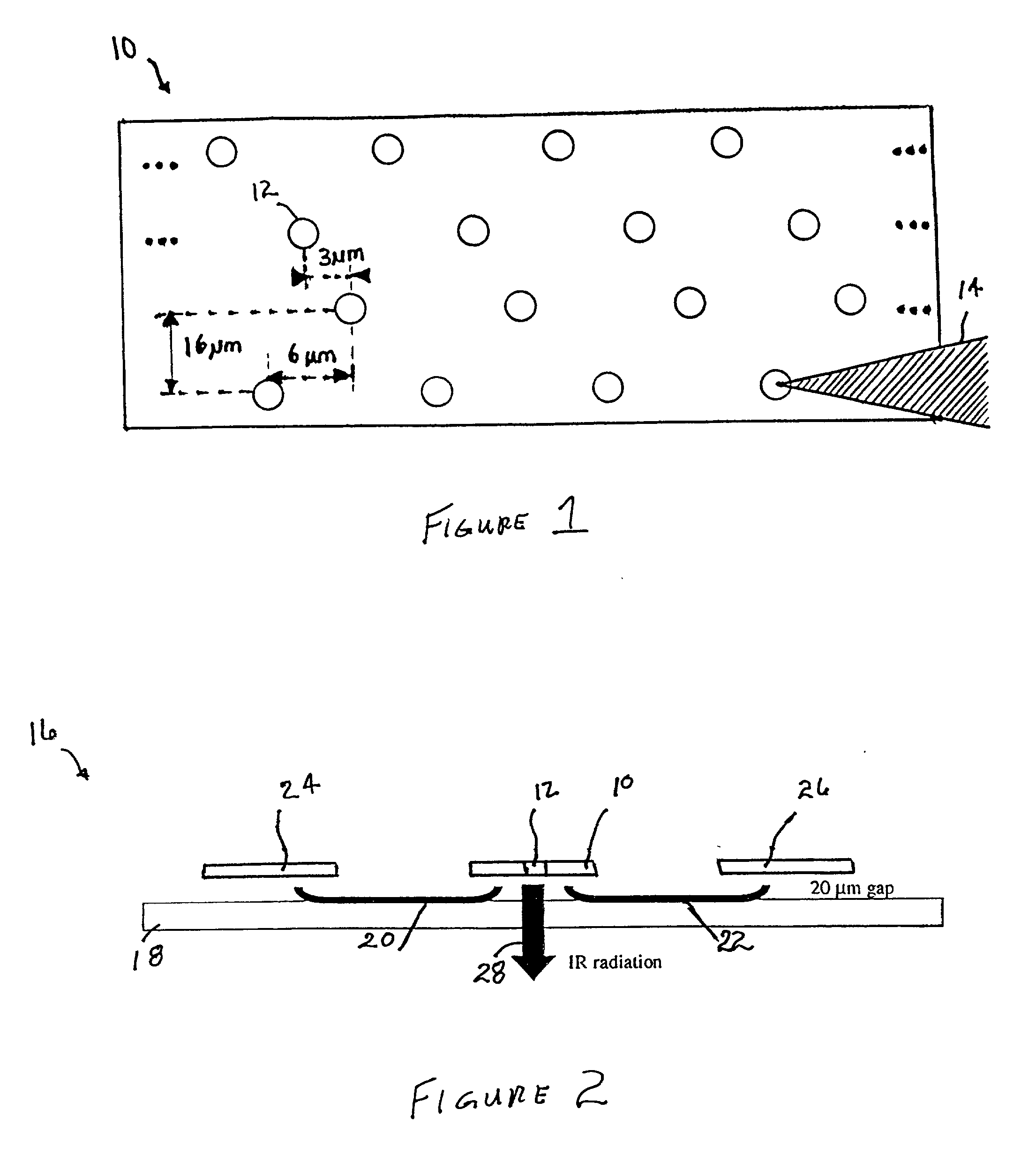
[0081] Turning to the calibration process, it is noted that in a first embodiment, calibration of lasers 12 of printbar 10 is accomplished by sensing and calibrating a single laser at a time. Particularly, sensors (34, 34', 53, 68, 74) are sufficiently sized to be placed in front of all lasers 12 of printbar 10. In one calibration scheme, the imaging device is not being used to print an image during calibration. Rather, the calibration process takes place during a time when image processing is not occurring.

[0082] In the embodiment describing the laser printbar, it is assumed sensors 53, 68, 70 are rectangular sensors of approximately 4 cm by 200 micrometers, which is large enough to intercept 100% of the laser beams diverging from printbar 10, for a substantially 4 cm-long laser array. The typical divergence of the VCSEL's beam was noted to be smaller than 20.degree..

[0083] The transparency of the amorphous silicon film ensures sufficient laser radiation to exit from the sensor to ...


PUM


Abstract

A hybrid structure or device is provided wherein carried on a single substrate is at least one micro-spring interconnect having an elastic material that is initially fixed to a surface of the substrate, an anchor portion which is fixed to the substrate surface and a free portion. The spring contact is self-assembling in that as the free portion is released it moves out of the plane of the substrate. Also integrated on the substrate is a sensor having an active layer and contacts. The substrate and sensor may be formed of materials which are somewhat partially transparent to light at certain infrared wavelengths. The integrated sensor/spring contact configuration may be used in an imaging system to sense output from a light source which is used for image formation. The light source may be a laser array, LED array or other appropriate light source. The sensor is appropriately sized to sense all or some part of light from the light source. The sensor may also be sufficiently transparent so that light is not blocked from its emission path, with a contrast ratio such that it only absorbs a small fraction of light passing therethrough. An additional characteristic is that the manufacturing process is compatible with the manufacturing process for the micro-spring interconnects. Data from the sensor is used as light source correction information. This information is provided to a calibration configuration which allows for calibration of high-speed systems.

Description

[0001] 1. Field of the Invention[0002] This invention relates to imaging systems using a sensor element to control the emission of at least some of the light of one or more light-emitting sources. In particular, this invention is directed to architectures, characteristics and methods of integration of a light sensor configuration with different light sources, using micro-fabricated metal spring contacts.[0003] 2. Technical Background[0004] Image printbars which are used in imaging systems are well known in the art. Such printbars are generally comprised of a linear array of a plurality of discreet, light-emitting sources. Examples of such printbars include light-emitting diodes and lasers. A method of forming lasers in semiconductor material, which may be used in the formation of laser printbars has been taught by, for example, U.S. Pat. No. 5,978,408 to Thornton, entitled, "Highly Compact Vertical Cavity Surface Emitting Lasers", issued Nov. 2, 1999; and U.S. Pat. No. 5,843,802 to ...

Claims


Application Information

Patent Timeline
IPC IPC(8): B41J2/45B41J2/44B41J2/455B81B3/00H01L25/075H01L31/101H01L31/105H01S5/02H01S5/026H01S5/40
CPCH01S5/4025B41J2/45H01L25/0753H01L31/1016H01L31/1055H01L2924/3011H01L2924/0002H01S5/02H01S5/0262H01L2924/00
Inventor LEMMI, FRANCESCOCHUA, CHRISTOPHER L.MEI, PINGLU, JENGPINGFORK, DAVID K.MCINTYRE, HARRY J.
Owner XEROX CORP
Why Eureka
Try Eureka