Method of forming a substrate-triggered SCR device in CMOS technology

Inactive Publication Date: 2003-04-24
KER MING DOU +2
View PDF8 Cites 18 Cited by
  • Summary
  • Abstract
  • Description
  • Claims
  • Application Information

AI Technical Summary

Benefits of technology

0019] It is an advantage of the present invention that in the design and method for making the ESD protection SCR device, the substrate-triggered current I.sub.trig flows into or flows out from the P-type substrate through the trigger node. Therefore, the lateral SCR is triggered on into its latch state and leads to a much lower switching voltage in the SCR device. With a much lower switching voltage in the SCR device, the total layout area of the ESD protection circuit may be reduced, and the turn-on spe

Problems solved by technology

With respect to this issue, heat dissipation issues become paramount.
If the LSCR device 14 does not trigger on in a sufficiently rapid manner, the secondary protection circuit 15 may be damaged by the ESD energy.
Also, if the secondary protection circuit 15 is not properly designed, it will cause window failure in ESD test scanning from a low voltage to a high voltage.
Such input ESD protection circuits were found to pass ESD stresses with low voltage levels or high voltage levels, but failed under tests with mid-ranged ESD stress voltage levels.
The thinner gate oxides of the input stages in very deep submicron CMOS ICs are therefore effec

Method used


Image

  • Method of forming a substrate-triggered SCR device in CMOS technology
  • Method of forming a substrate-triggered SCR device in CMOS technology
  • Method of forming a substrate-triggered SCR device in CMOS technology

Examples


Embodiment Construction

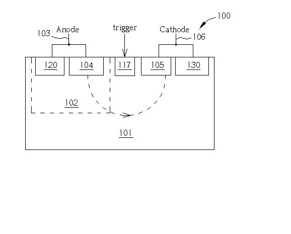
[0060] Please refer to Fig.5(a) to 5(b). Fig.5(a) is a cross-sectional schematic diagram of a P-type substrate-triggered SCR (P_STSCR) device 100 according to the present invention. Fig.5(b) is a diagram of a corresponding symbol for the P_STSCR device 100. As shown in Fig.5(a), the P_STSCR device 100 is made in a P-type silicon substrate 101. The P_STSCR device 100 comprises an N-well 102. A P.sup.+ region 104 and an N.sup.+ region 120 in the N-well 102 are electrically connected to an anode 103. A P.sup.+ region 130 and an N.sup.+ region 105 in the P-type substrate 101 are electrically connected to a cathode 106. A P.sup.+ diffusion 117 is use as a trigger node of the P_STSCR device 100. The P.sup.+ region 104, the N-well 102, the P-type substrate 101 and the N.sup.+ region 105 together form an LSCR device. When a current flows from the trigger node (i.e., the inserted P.sup.+ diffusion 117) into the P-type substrate 101, the lateral SCR is triggered on into its latch state to pro...


PUM


Abstract

Abstract of Disclosure A P_STSCR structure includes a P-type substrate, an N-well in the P-type substrate, a first N+ diffusion region located in the P-type substrate connected to the cathode, a second P+ diffusion region located in the N-well connected to the anode, and a third P+ diffusion region as a trigger node located in the P-type substrate and between the first N+ diffusion region and the second P+ diffusion region. A lateral SCR device including the second P+ diffusion region, the N-well, the P-type substrate and the first N+ diffusion region is thereby formed. When a current flows from the trigger node into the P-type substrate, the lateral SCR device is triggered on into its latch state to discharge ESD current. Since the present invention utilizes a substrate-triggered current Itrig flowing into or flowing out from the P-type substrate or the N-well through the inserted trigger node, a much lower switching voltage in the SCR device is obtained.With such a lower switching voltage in the SCR device, the total layout area of the ESD protection circuit can be reduced, and the turn-on speed of SCR device is further improved to quickly discharge ESD current.ESD current flowing through surface channels, and heat dissipation issues, are avoided, while presenting no increase to the overall complexity and difficulty of CMOS IC manufacturing.

Description

Cross Reference To Related Applications[0001] This application is a division of application Serial No. 09 / 682,400 filed Aug. 30, 2001Background of Invention[0002] 1.Field of the Invention[0003] The present invention provides a method for making a silicon controlled rectifier(SCR) device utilizing in electrostatic discharge (ESD) protection circuits. In particular, a silicon controlled rectifier device structure with substrate-triggered effect.[0004] 2.Description of the Prior Art[0005] With the continued scaling down of semiconductor integrated circuit (IC) devices, the present trend is moving towards production of semiconductor integrated circuits having very small sizes in the advanced sub-quarter-micron CMOS technologies. It is consequently increasingly important to build electrostatic discharge (ESD) protection circuits on the chip to protect the devices and circuits of the IC against ESD-related damage. The ESD robustness of commercial IC products is generally needed to be high...

Claims


Application Information

Patent Timeline
IPC IPC(8): H01L21/332H01L27/02H01L29/74
CPCH01L27/0262H01L29/7436H01L29/66393
Inventor KER , MING-DOUCHEN , TUNG-YANGTANG , TIEN-HAO
Owner KER MING DOU
Why Eureka
Try Eureka