

Display device and method for driving the same
a display device and a technology for driving the same, applied in the direction of instruments, static indicating devices, etc., can solve the problems of large noise, slow image displaying speed, and limited speed for transferring signals from the frame memory to the pixel portion
- Summary
- Abstract
- Description
- Claims
- Application Information
AI Technical Summary
Problems solved by technology
Method used
Image

Examples
embodiment 1
[0085] (Embodiment 1)
[0086] This embodiment describes a construction of a display in which device digital video signals are stored in a memory, and analog-converted and input to a pixel portion.
[0087] FIG. 3 is a block diagram showing a construction of this embodiment.
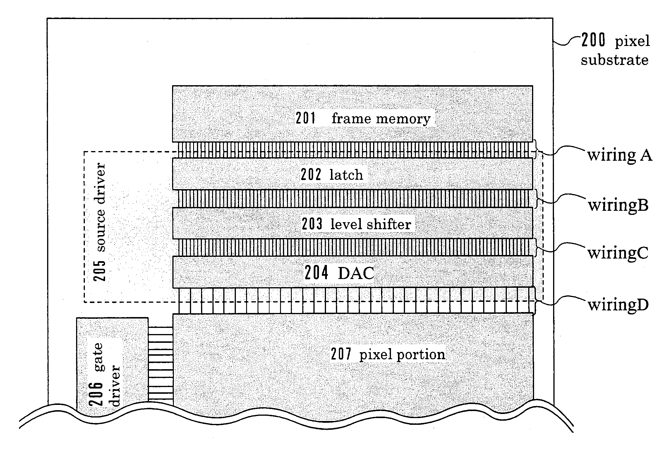
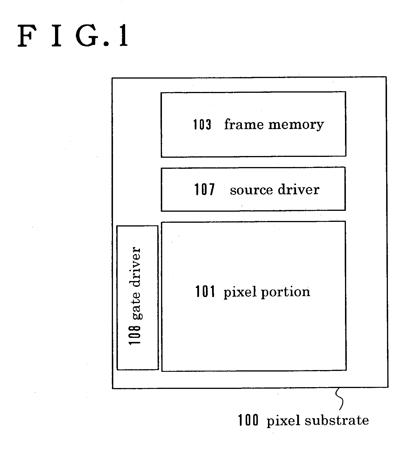
[0088] In FIG. 3, a display device has a frame memory 201, a source driver 205, a gate driver 206 and a pixel portion 207, which are formed on a pixel substrate 200 having an insulating surface. In the frame memory 201, digital video signals input from the outside of the display device are stored.
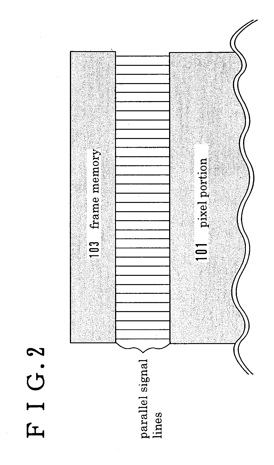
[0089] Here, the number of wirings A to C is equal to the number of pixels.times.bits for one row in the case of RGB color. The number of wirings D is equal to the number of pixels for one row. That is, in this case, image data for one row can be sent out simultaneously.
[0090] As described in the embodiment, data for one row of pixel does not have to be stored in one row of frame memory and may be data for one row of pixels or...
embodiment 2
[0111] (Embodiment 2)
[0112] In this embodiment, processes of a formation of a structure shown in the first embodiment, in which a display portion, a driver circuit and a memory cell are formed in one body is explained below. Note that the driver circuit portion and the memory cell portion are referred to as a CMOS circuit that is a basic unit thereof.
[0113] Further, transistors that compose pixels are referred as to a transistor 454 shown in FIG. 14.
[0114] As for the pixels, only a TFT for writing, a source signal, and a storage capacitor are shown.
[0115] First, as shown in FIG. 15A, a base film 3002 consisting of an insulating film such as a silicon oxide film, a silicon nitride film or a silicon oxynitride film is formed on a substrate 3001 consisting of glass such as barium borosilicate glass or alumino borosilicate glass represented by #7059 glass and #1737 glass of Coning Corporation. For example, a silicon oxynitride film 3002a formed from SiH.sub.4, NH.sub.3 and N.sub.2O by t...
embodiment 3
[0148] (Embodiment 3)
[0149] The following description exemplifies the fabrication process in case where the invention is adapted to a reflection type liquid crystal display apparatus, which is different from the liquid crystal display apparatus of the embodiment 2.
[0150] According to the embodiment 2, an active matrix substrate shown in FIG. 18A (similar to the one shown in FIG. 17A) is prepared. Subsequently, a resin film is formed as a third interlayer insulating film 3201 after which a contact hole is bored in the pixel electrode portion and a reflection electrode 3202 is formed there. It is desirable to use a material having an excellent reflectivity, such as a film essentially consisting of Al or Ag or the lamination of those films, as the reflection electrode 3202.
[0151] An opposing substrate 3056 is prepared. In this embodiment, an opposing electrode 3205 is formed by patterning on the opposing substrate 3056. The opposing electrode 3205 is formed as a transparent conductive ...
PUM
 Abstract
Description
Claims
Application Information