Position sensitive solid state detector with internal gain

a solid state detector and gain technology, applied in the direction of radiation intensity measurement, instruments, x/gamma/cosmic radiation measurement, etc., can solve the problems of limiting the real-time dynamic range of the detector for detecting sequential pulses of radiation, introducing optical losses, and limited quantum efficiency of the photocathode material

Inactive Publication Date: 2003-05-01
SCI WARES +1
View PDF6 Cites 24 Cited by
  • Summary
  • Abstract
  • Description
  • Claims
  • Application Information

AI Technical Summary

Problems solved by technology

However, they are limited by the quantum efficiency of the photocathode material, which in practice is typically in the range of 10-20%.
Both methods introduce optical losses when the detector is used with proximity-focused scintillator arrays.
Detectors that use microchannel plate structures for internal amplification suffer from a localized dead time on the order of 10-100 milliseconds, which severely limits the realizable dynamic range of the detector for detecting sequential pulses of radiation.
Vacuum tube detectors are also frequently constructed in a round enclosure, which is inefficient for tiling to cover large areas.
Furthermore, magnetic fields that are not parallel to the electron transit path inside the vacuum enclosure will always cause geometric distortion in a position sensitive readout and may affect gain as well.
However, because they are photodiodes that have no internal gain, all of these detectors are limited to applications that have relatively low bandwidth requirements and a relatively high background when compared to what is possible with avalanche photodiodes.
There are a number of reasons why the prior art methods for extracting position sensitive information from photodiodes cannot be directly extended to work with APDs.
The contact method also affects the package design, which can in turn affect the usability of the detector in tiling applications.
The problem of cross-talk between pixels can significantly complicate the signal readout, especially when energy resolution of the signal is important, and reducing the pixel size to improve resolution tends to increase cross talk problems.
As pixel size is decreased to improve spatial resolution, the ratio of active area to physical device area decreases, which can significantly reduce the amount of signal collected, which adversely affects signal to noise ratio as well as energy resolution.
The risk that fabricated devices will contain or develop dead or poorly functioning pixels adversely affects the manufacturing process yield as well as the value of the manufactured product.
Furthermore, as the number of pixels is increased, the complexity and cost Of the readout electronics also increases, especially in applications such as PET where coincidence determinations must be made using signals that extend over a large number of pixels.
Furthermore, the internal gain mechanism in APDs does not introduce a localized dead time that would limit dynamic range for detecting sequential events at the same position of incidence in the same way that microchannel plate based vacuum detectors are limited.

Method used


Image

  • Position sensitive solid state detector with internal gain
  • Position sensitive solid state detector with internal gain
  • Position sensitive solid state detector with internal gain

Examples


Embodiment Construction

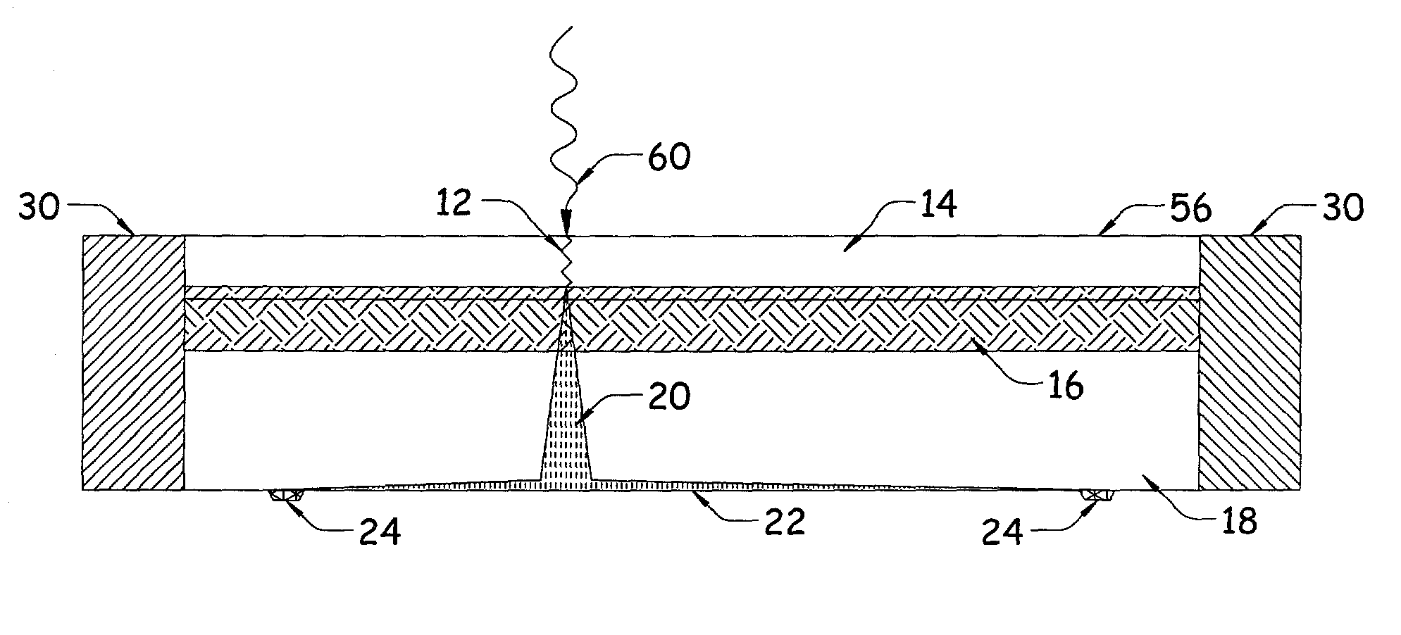
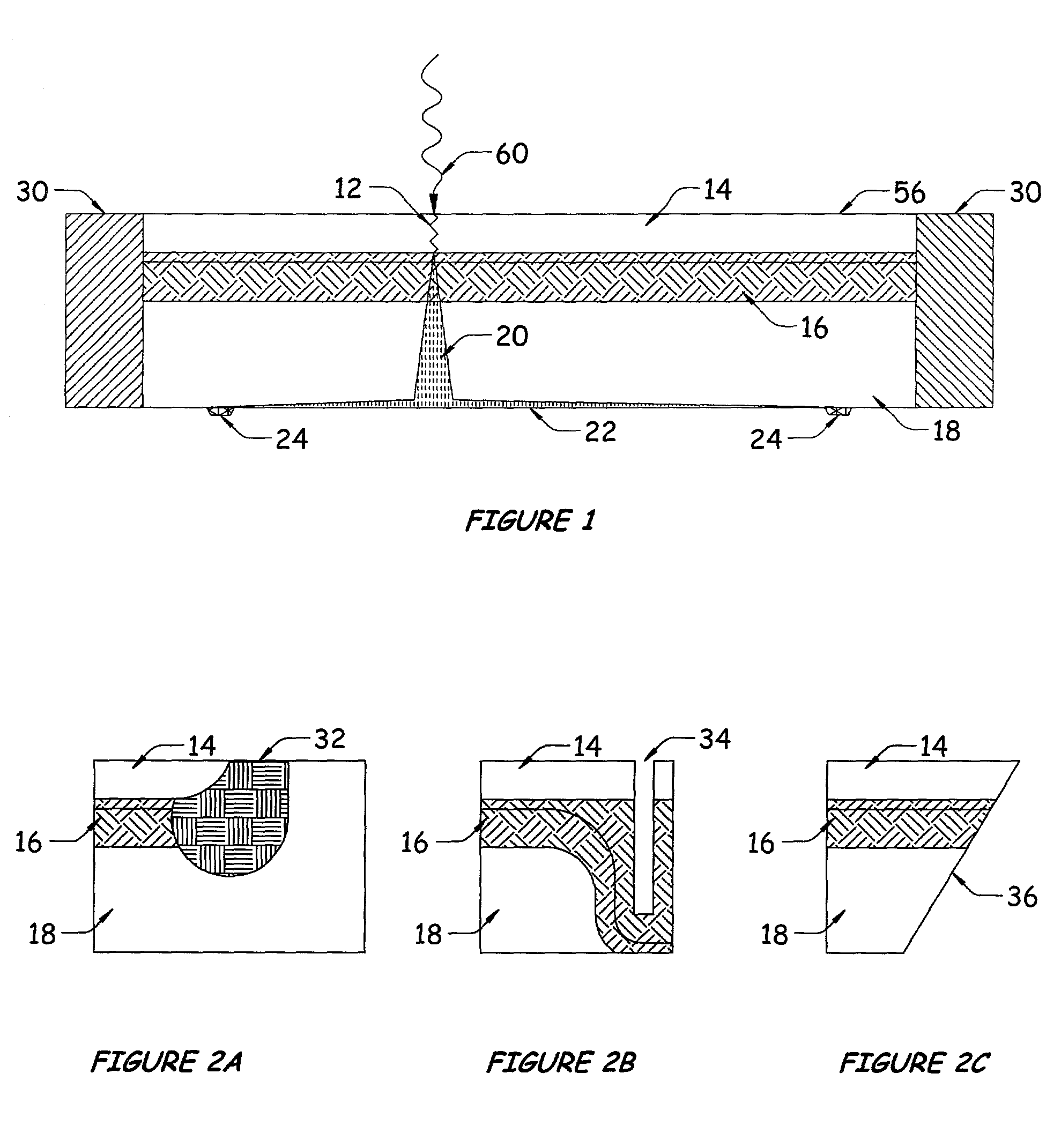
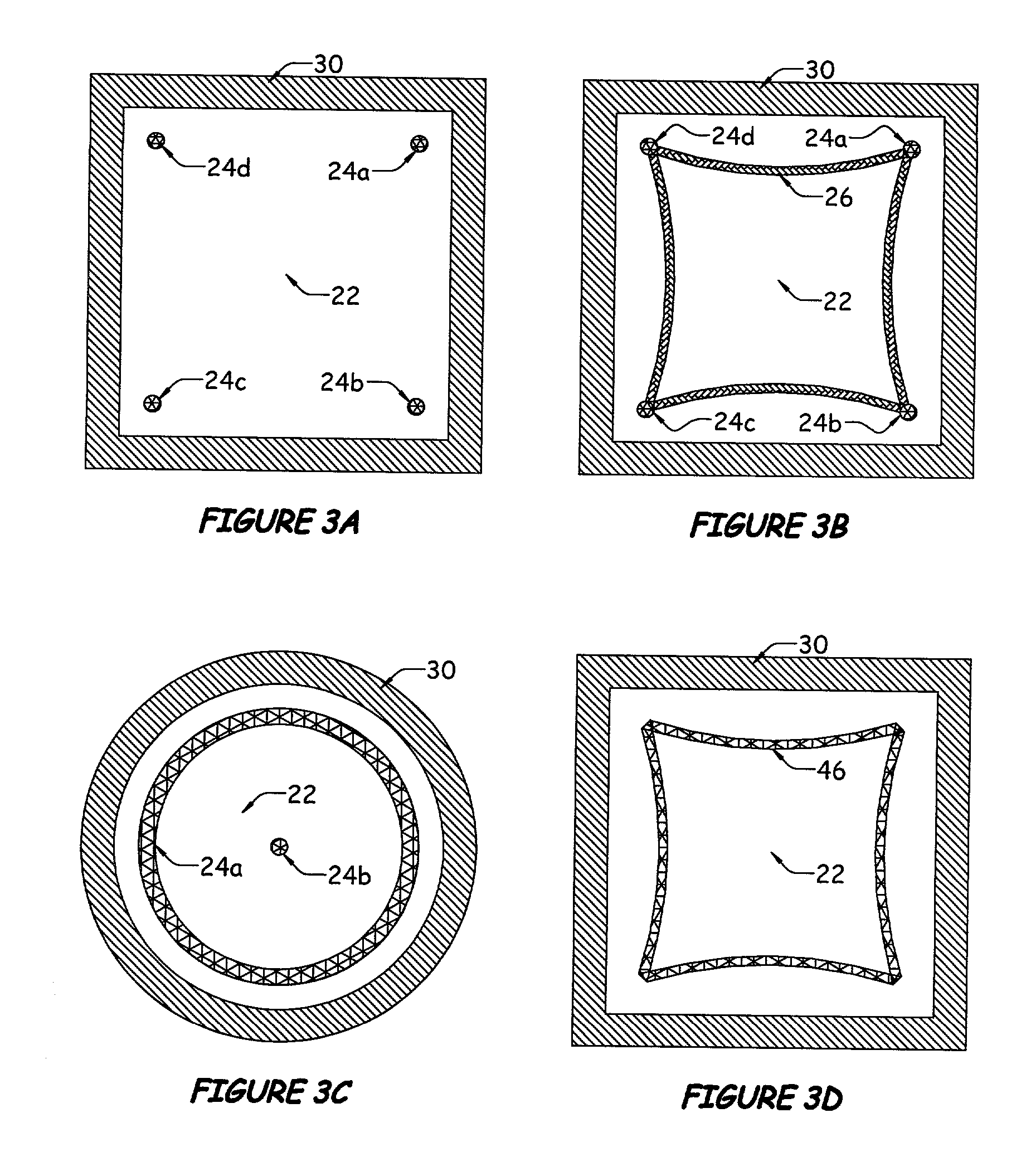
[0051] In a typical embodiment, a large area APD is fabricated in the usual way. It can be beneficial to the spatial resolution performance of the detector to minimize the thickness of the undepleted material on both sides of the depletion region 16, especially on the input side of the detector 14, in order to minimize the spread of minority carriers 12 produced by the input signal 60. In a preferred embodiment, an n silicon substrate 18 is doped with p materials using a deep diffusion process. A field spreading structure 30 such as a guard ring 32, diffused bevel 34, or mechanical bevel 36 is incorporated into the semiconductor material to avoid edge breakdown under high reverse bias. Other field spreading structures are possible and are considered to be within the scope of this invention. Prior to applying a passivation layer to the cathode side of the device, a photomask is applied to mask off a contact pattern. The contact pattern can be somewhat arbitrary, but it is necessary t...


PUM


Abstract

The present invention is a solid state detector that has internal gain and incorporates a special readout technique to determine the input position at which a detected signal originated without introducing any dead space to the active area of the device. In a preferred embodiment of the invention, the detector is a silicon avalanche photodiode that provides a two dimensional position sensitive readout for each event that is detected.

Description

[0002] 1. Field of Invention[0003] This invention describes methods of obtaining position of incidence information from solid state devices, such as avalanche photodiodes, without introducing any dead space to the detector's active area.[0004] 2. Discussion of Prior Art[0005] Many applications in science and industry require detectors that are capable of reporting time and position of incidence information for discrete quantum units of radiation such as single photons and beta particles. A single photon is understood to be a unit of radiation with an energy described by E=hc / .lambda., where .lambda. is the wavelength of the radiation. In some cases it is most expedient to convert a high energy photon into a group of multiple lower energy photons and then detect the group of lower energy photons as a single event corresponding to the lower energy photons. This is typically achieved using fluorescent materials such as scintillators.[0006] Detectors for these applications will ideally ...

Claims


Application Information

Patent Timeline
Patent Type & Authority Applications(United States)
IPC IPC(8): G01TG01T1/24H01L27/14H01L31/00H01L31/0232H01L31/062H01L31/107H01L31/113H01L31/115
CPCG01T1/247G01T1/208
Inventor KARPLUS, ERICFARRELL, RICHARDSHAH, KANAI
Owner SCI WARES
Why Eureka
Try Eureka