Resistance changeable device for data transmission system

Inactive Publication Date: 2003-05-01
RENESAS ELECTRONICS CORP
View PDF0 Cites 20 Cited by
  • Summary
  • Abstract
  • Description
  • Claims
  • Application Information

AI Technical Summary

Benefits of technology

0011] An object of the present invention is to provide, with due consideration to the drawbacks of the conventional data transmission systems, a resistance changeable device in which a resistance value of a termination resistor disposed on the inside of a semiconductor chip is adjustable so as to reduce both a manufac

Problems solved by technology

Therefore, in cases where a plurality of termination resistors 14 disposed on the outside of the receiving end device 13 are connected to all input terminals of the receiving end device 13 respectively, problems have arisen that the number of constituent elements disposed on a substrate (or a semiconductor chip), on which the receiving end device is disposed, is increased, the manufacturing cost of the data transmission system is increased and an element disposing area of the substrate is increased.
However, in this case, because it is difficult to uniformly form the termination resist

Method used


Image

  • Resistance changeable device for data transmission system
  • Resistance changeable device for data transmission system
  • Resistance changeable device for data transmission system

Examples


embodiment 1

[0045] EMBODIMENT 1

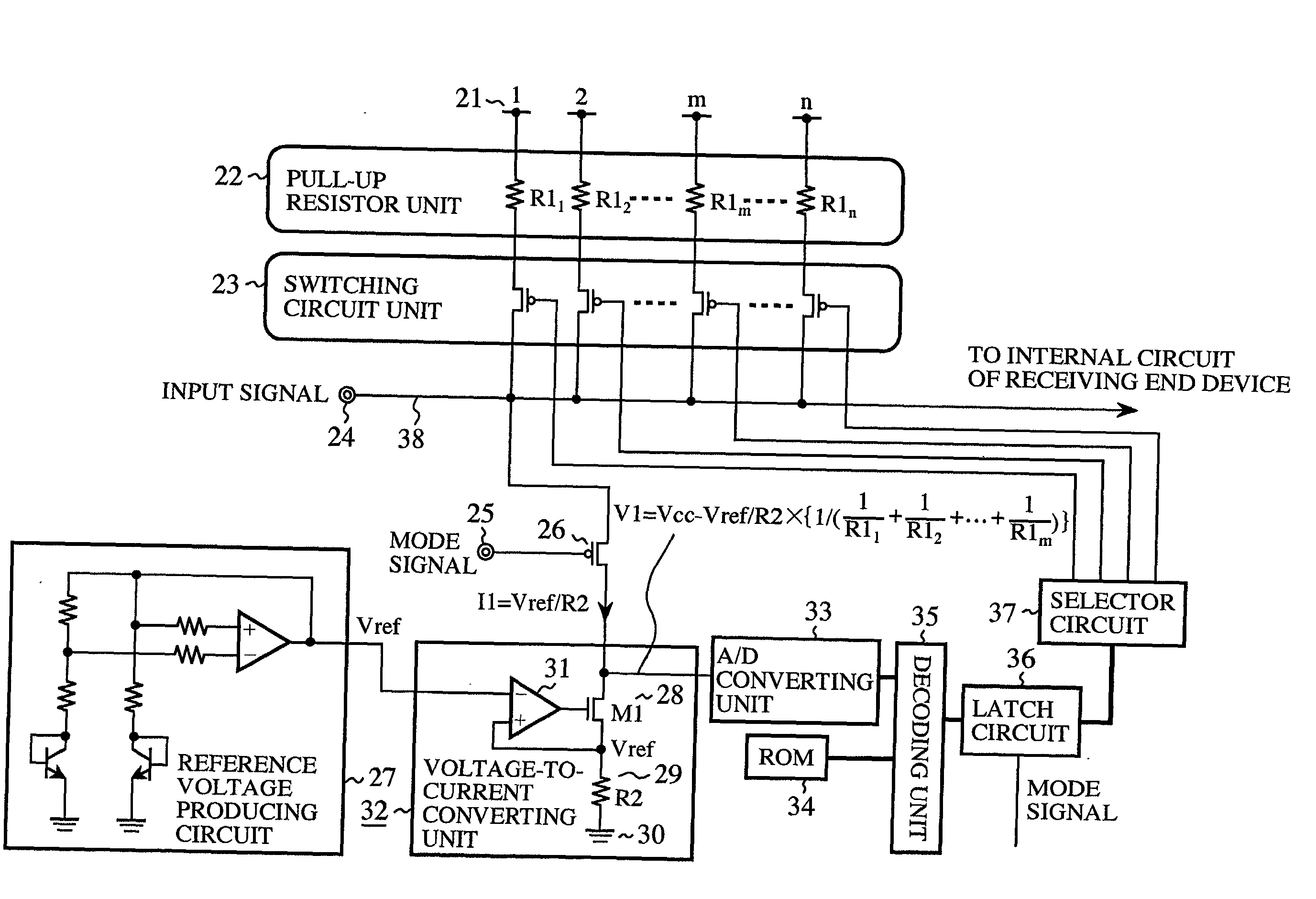
[0046] FIG. 1 is a circuit view of a resistance changing device according to a first embodiment of the present invention. In FIG. 1, 21 indicates an electric power source (or a high electric potential source) set to a source voltage Vcc. 22 indicates a pull-up resistor unit in which a plurality of resistive elements (for example, resistors) tried to be formed in the same size as each other are disposed in parallel to each other. The resistive elements have resistance values R1.sub.1, R1.sub.2, - - - and R.sub.1, (n denotes an integral number equal to or higher than 2) slightly different from each other, and the resistance values of the resistive elements are distributed around a desired resistance value R1. One end of each resistive element is connected to the electric power source 21. 23 indicates a switching circuit unit in which a plurality of P-channel metal oxide semiconductor (PMOS) transistors (or a plurality of switches) are disposed in parallel to each ot...

embodiment 2

[0065] EMBODIMENT 2

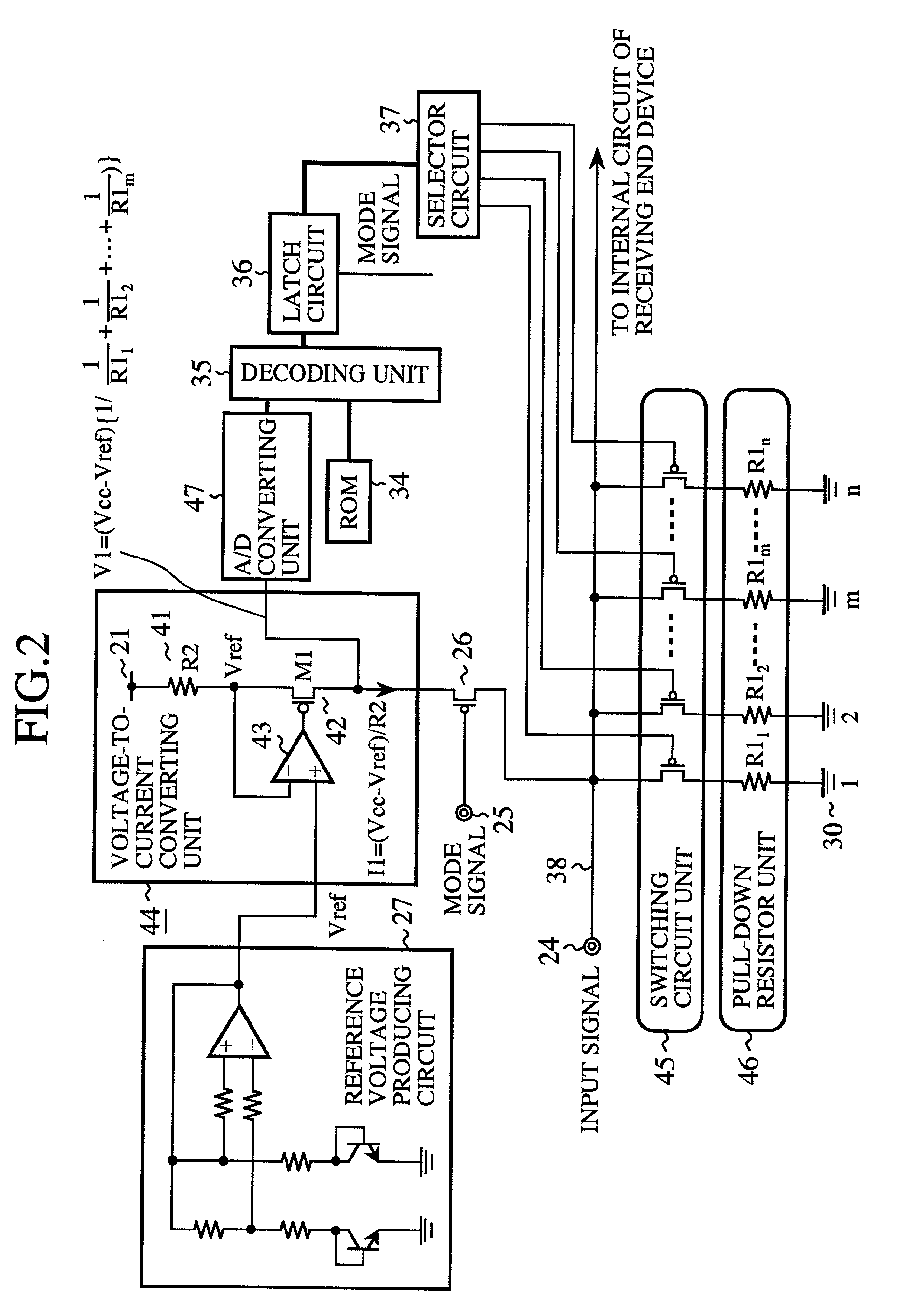
[0066] FIG. 2 is a circuit view of a resistance changing device according to a second embodiment of the present invention. The constituent elements, which are the same as those shown in FIG. 1, are indicated by the same reference numerals as those of the constituent elements shown in FIG. 1, and additional description of those constituent elements is omitted.

[0067] In FIG. 2, 41 indicates an external resistor having a resistance value R2 which is disposed on the outside of the semiconductor chip. One end of the external resistor 41 is connected to the electric power source 21. 42 indicates a PMOS transistor. A source of the PMOS transistor 42 is connected to the other end of the external resistor 41. 43 indicates an operational amplifier. A non-inversion (+) input terminal of the operational amplifier 43 is connected to the reference voltage producing circuit 27, an inversion (-) input terminal of the operational amplifier 43 is connected to a node between the ext...

embodiment 3

[0086] EMBODIMENT 3

[0087] FIG. 3 is a circuit view of a resistance changing device according to a third embodiment of the present invention. The constituent elements, which are the same as those shown in FIG. 1, are indicated by the same reference numerals as those of the constituent elements shown in FIG. 1, and additional description of those constituent elements is omitted.

[0088] In FIG. 3, 22a indicates a pull-up resistor unit of a system A in which a plurality of resistive elements tried to be formed in the same size as each other are disposed in parallel to each other. The resistive elements have resistance values R1a.sub.1, R1a.sub.2, - - - and R1a.sub.n (n denotes an integral number equal to or higher than 2) slightly different from each other, and the resistance values of the resistive elements are distributed around a desired resistance value R1a. One end of each resistive element is connected to the electric power source 21. 23a indicates a switching circuit unit of the s...


PUM


Abstract

On a semiconductor chip, ends of a plurality of resistive elements of a pull-up resistor unit disposed in parallel to each other are connected to a power source, other ends of the resistive elements are connected to a line connecting a signal input terminal and a receiving end device disposed on the semiconductor chip, and the line is connected to the ground through an external resistor disposed on the outside of the semiconductor chip. A current flows from the power source to the ground, and a node voltage depending on a resistance value of the external resistor and a composite resistance of the pull-up resistor unit is applied to a node between the line and the external resistor. The composite resistance of the pull-up resistor unit functioning as a termination resistor is corrected to an expected value according to the node voltage.

Description

BACKGROUND OF THE INVENTION[0001] 1. Field of the Invention[0002] The present invention relates to a resistance changeable device used for a data transmission system having a plurality of data transmission channels, and more particularly to a resistance changeable device used for a receiving end device which is used for a data transmission system requiring of the adjustment of an input impedance. Also, the present invention relates to a resistance changeable device usable for a differential output circuit such as a low voltage differential signaling (LVDS) system which is used for a notebook-sized personal computer and is characterized by data transmission at high speed, low voltage and low noise.[0003] 2. Description of Related Art[0004] FIG. 6 is a view of an equivalent circuit of a conventional data transmission system, and FIG. 7 is a view of an equivalent circuit of another conventional data transmission system. In FIG. 6 and FIG. 7, 1 indicates a transmission line formed of a ...

Claims


Application Information

Patent Timeline
IPC IPC(8): H03K19/0175H04L25/02
CPCH04L25/0272H04L25/0292H04L25/028H04L25/0278
Inventor NAGANO, HIDEO
Owner RENESAS ELECTRONICS CORP
Why Eureka
Try Eureka