Lightly-insitu-doped amorphous silicon applied in DRAM gates

a technology of amorphous silicon and dram gates, which is applied in the direction of basic electric elements, semiconductor/solid-state device manufacturing, electric apparatus, etc., can solve the problems of critical boron penetration and thin thickness of gate oxide 104

Inactive Publication Date: 2003-05-15
PROMOS TECH INC
View PDF0 Cites 10 Cited by
  • Summary
  • Abstract
  • Description
  • Claims
  • Application Information

AI Technical Summary

Benefits of technology

0012] An objective of the present invention is to provide a method for manufacturing a semiconductor device to

Problems solved by technology

As the integration density of semiconductors increases rapidly, the thickness of the gate oxide 104 becomes thinner and

Method used


Image

  • Lightly-insitu-doped amorphous silicon applied in DRAM gates
  • Lightly-insitu-doped amorphous silicon applied in DRAM gates
  • Lightly-insitu-doped amorphous silicon applied in DRAM gates

Examples


Embodiment Construction

[0020] The present invention is to provide a method for manufacturing a semiconductor device, and the semiconductor device has a substrate. The substrate includes a first conductive region of a first conductivity type, a second conductive region of a second conductivity type, and an oxide is formed on the substrate.

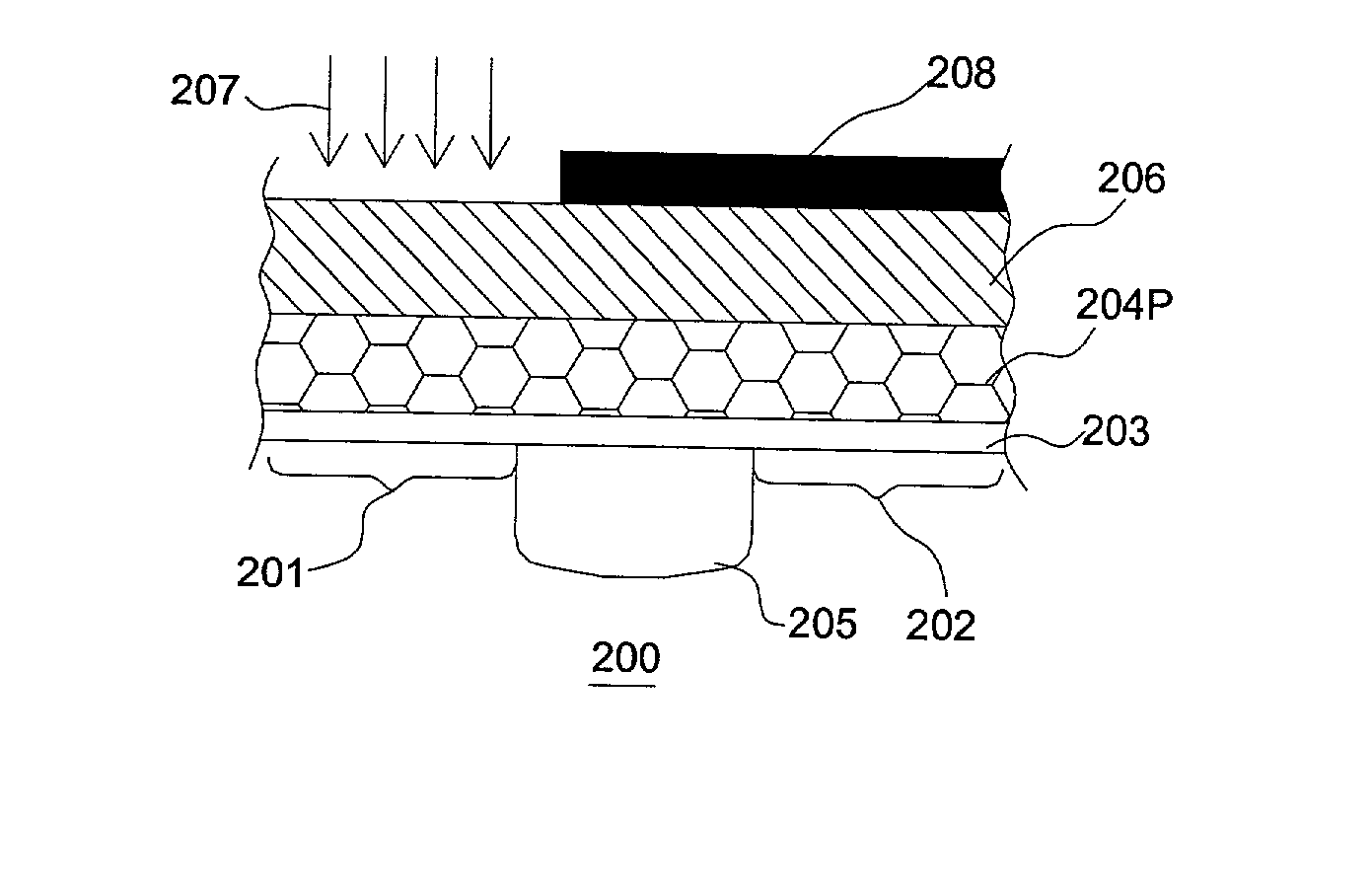
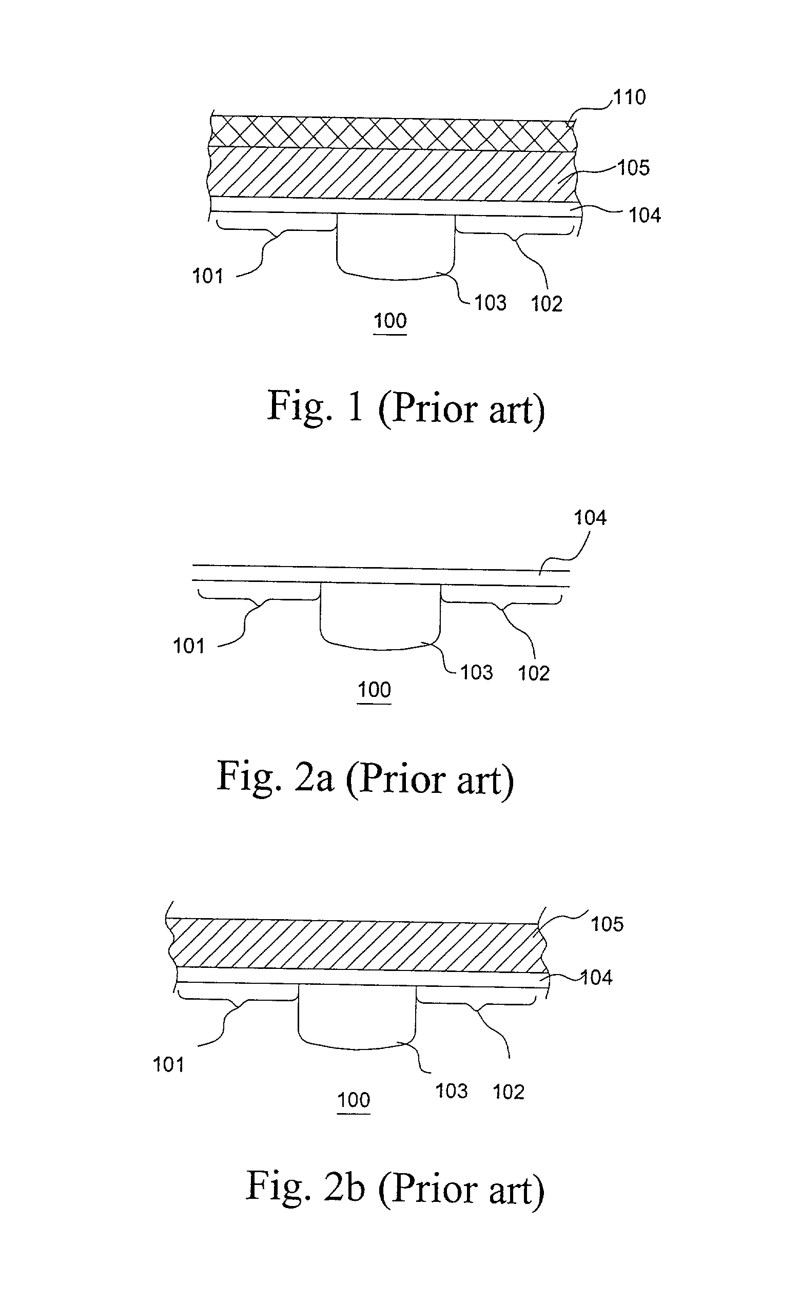
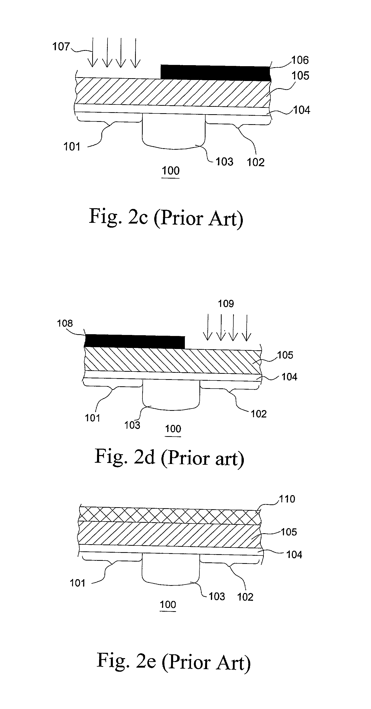
[0021] Please refer to FIG. 3a, a substrate 200 includes a region 201 which an NMOSFET is to be formed and a region 202 which a PMOSFET is to be formed. The regions 201 and 202 are separated by a shallow trench isolation 205, and a gate oxide 203 is on the substrate 200.

[0022] Afterwards, in a preferred embodiment, a lightly-doped amorphous silicon layer 204A is formed over the gate oxide 203, as shown in FIG. 3b. The "lightly-doped" indicates that the doped concentration in this stage is lighter than the finalized doped concentration of the region 201 and region 202.

[0023] The lightly-doped amorphous silicon layer 204A is usually formed by a chemical vapor deposition met...


PUM


Abstract

The present invention forms a polysilicon by first forming then thermally processing a lightly in-situ doped amorphous silicon layer, thus suppressing boron penetration and lateral diffusion of N-type and P-type impurities.

Description

[0001] The present invention relates to lightly-insitu-doped amorphous silicon, and particularly to lightly-insitu-doped amorphous silicon applied in DRAM gates.[0002] A Complementary Metal Oxide Semiconductor transistor (CMOS) includes an N-channel Metal Oxide Semiconductor Field Effect Transistor (NMOSFET) and a P-channel MOSFET (PMOSFET). If the CMOS is a twin wells construction, the twin wells are N-type and P-type well respectively. The CMOS, having advantages of low power assumption and high speed, is extensively used in many memory and logic circuits of semiconductor devices, such as a control transistor of a Dynamic Random Access Memory (DRAM).[0003] Because there are electrodes for the NMOSFET and the PMOSFET of the CMOS, the CMOS includes P-type and N-type doped gates. Therefore, the N-type impurities, such as arsenic and phosphorus, and the P-type impurities, such as boron and boron difluoride, are respectively implanted into regions which NMOSFET and PMOSFET are to be fo...

Claims


Application Information

Patent Timeline
IPC IPC(8): H01L21/8238
CPCH01L21/823842
Inventor HSU, CHIA-FUCHENG, CHIN-CHENG
Owner PROMOS TECH INC
Why Eureka
Try Eureka