Programmable logic device and method of controlling clock signal thereof

a logic device and clock signal technology, applied in the direction of generating/distributing signals, pulse techniques, instruments, etc., can solve the problems of increasing the amount of generated heat, the rate of power consumption is a decisive factor, and the rate of power consumption has not reached a satisfactory level

Inactive Publication Date: 2003-06-12
FUJITSU LTD
View PDF0 Cites 12 Cited by
  • Summary
  • Abstract
  • Description
  • Claims
  • Application Information

AI Technical Summary

Problems solved by technology

In particular, the logic device is frequently utilized in a part of system serving as an interface with an external system where it is difficult to construct the part of system with a microprocessor unit or a digital signal processor.
However, when the logic device is applied to a system such as a mobile communication terminal or a portable telephone, a rate of power consumption is a decisive factor, in addition to the operation speed and the circuit scale, upon selecting a device.
When a programmable logic device is designed in a conventional manner, since the circuit size or the operation speed is regarded as a priority factor, the rate of power consumption has not reached a satisfactory level as compared with an LSI designed for a specific use.
In general, when the device of the rate of power consumption is large, the generated heat amount also is increased.
However, if the device is employed in the system such as a mobile communication terminal, to suppress the heat generation due to the electric power consumption becomes a more important factor.
That is, if a circuit device having a high heat generating nature is employed in a system, a cooling device is requested for guaranteeing the operation of the circuit, which leads to a cost increase in the system.
However, the clock signal itself is inevitably delivered to the

Method used


Image

  • Programmable logic device and method of controlling clock signal thereof
  • Programmable logic device and method of controlling clock signal thereof
  • Programmable logic device and method of controlling clock signal thereof

Examples


Embodiment Construction

[0047] Embodiments of the present invention will be hereinafter described with reference to drawings.

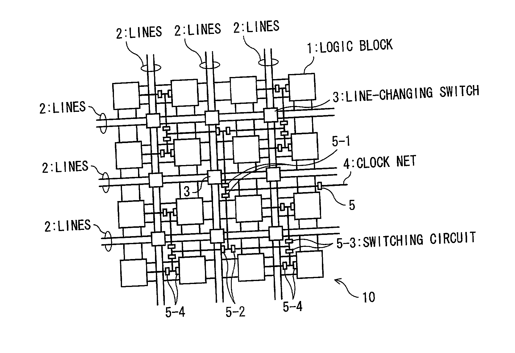
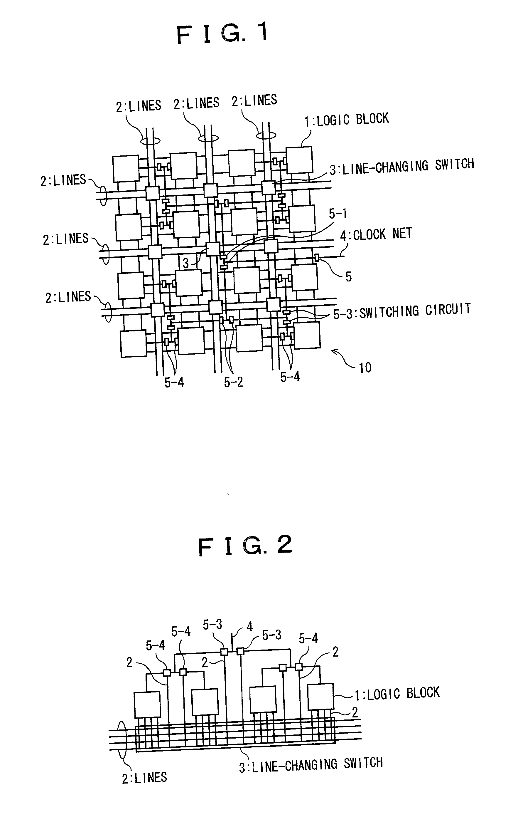
[0048] FIG. 1 is a circuit diagram showing a part of an FPGA as a programmable logic device according to a first embodiment of the present invention. As shown in FIG. 1, similarly to that shown in FIG. 8, an FPGA 10 is arranged to include a plurality (there are shown 16 blocks in FIG. 1) of arrayed logic blocks 1 for carrying out logical operation, lines 2 for connecting the logic blocks to one another, line-changing switches 3 as line-changing means for changing the state of changing (connection state) among the respective logic blocks through the lines 2 by programming.

[0049] Each of the logic blocks 1 is arranged to include elements such as flip-flops and so on which are operable in synchronism with a clock signal. The operation of the logic block 1 itself can be changed by programming. The lines 2 are composed of a plurality of lines extending in the longitudinal direction and th...


PUM


Abstract

An object of the present invention is to provide a programmable logic device which intends to reduce electric power consumption or heat generation sufficiently as a whole device while preventing a clock skew from being generated and retaining a processing speed of the device. To this end, according to the present invention, there is provided a device including logic blocks for carrying out logical operation, lines for connecting the logic blocks, line-changing means for changing the state of lines connecting the logic blocks by programming, a clock net for supplying a clock signal to each of the logic blocks, and clock control means for dynamically controlling switching between a clock signal supply mode and a clock signal stop mode for each logic block so that at least one non-active logic block of the logic blocks can be stopped from being supplied with the clock signal.

Description

[0001] 1) Field of the Invention[0002] The present invention relates to a programmable logic device suitable for use as a logic device such as an FPGA (Field Programmable Gate Array), a CPLD (Complex programmable Logic Device) in which the function thereof can be changed in accordance with a program. The present invention also relates to a method of controlling a clock signal supplied to the programmable logic device.[0003] 2) Description of the Related Art[0004] A programmable logic device represented by a device such as an FPGA or CPLD is a logic device of which operation can be changed in accordance with a program. The programmable logic device has an advantageous nature that makes it possible to handle various kind of problems such as specification change of the product which will be brought about at an early stage of product development. For this reason, recently, technology of the logic device is rapidly developed.[0005] Since the logic device tends to suffer from restriction ...

Claims


Application Information

Patent Timeline
IPC IPC(8): G06F15/80H01L21/82H01L21/822H01L27/04H03K19/177
CPCH03K19/17736H03K19/17784H03K19/1774
Inventor KUMAMOTO, NORICHIKA
Owner FUJITSU LTD
Why Eureka
Try Eureka