

Method of manufacturing silicon
a technology of silicon and production method, which is applied in the direction of crystal growth process, silicon compounds, chemistry apparatus and processes, etc., can solve the problems of affecting the productivity affecting the efficiency of the manufacturing process, and requiring a lot of effort, so as to achieve effective reduction of contamination caused by contact between the substrate and the molten silicon, and continuous deposition and recovery of silicon.
- Summary
- Abstract
- Description
- Claims
- Application Information
AI Technical Summary
Benefits of technology
Problems solved by technology
Method used
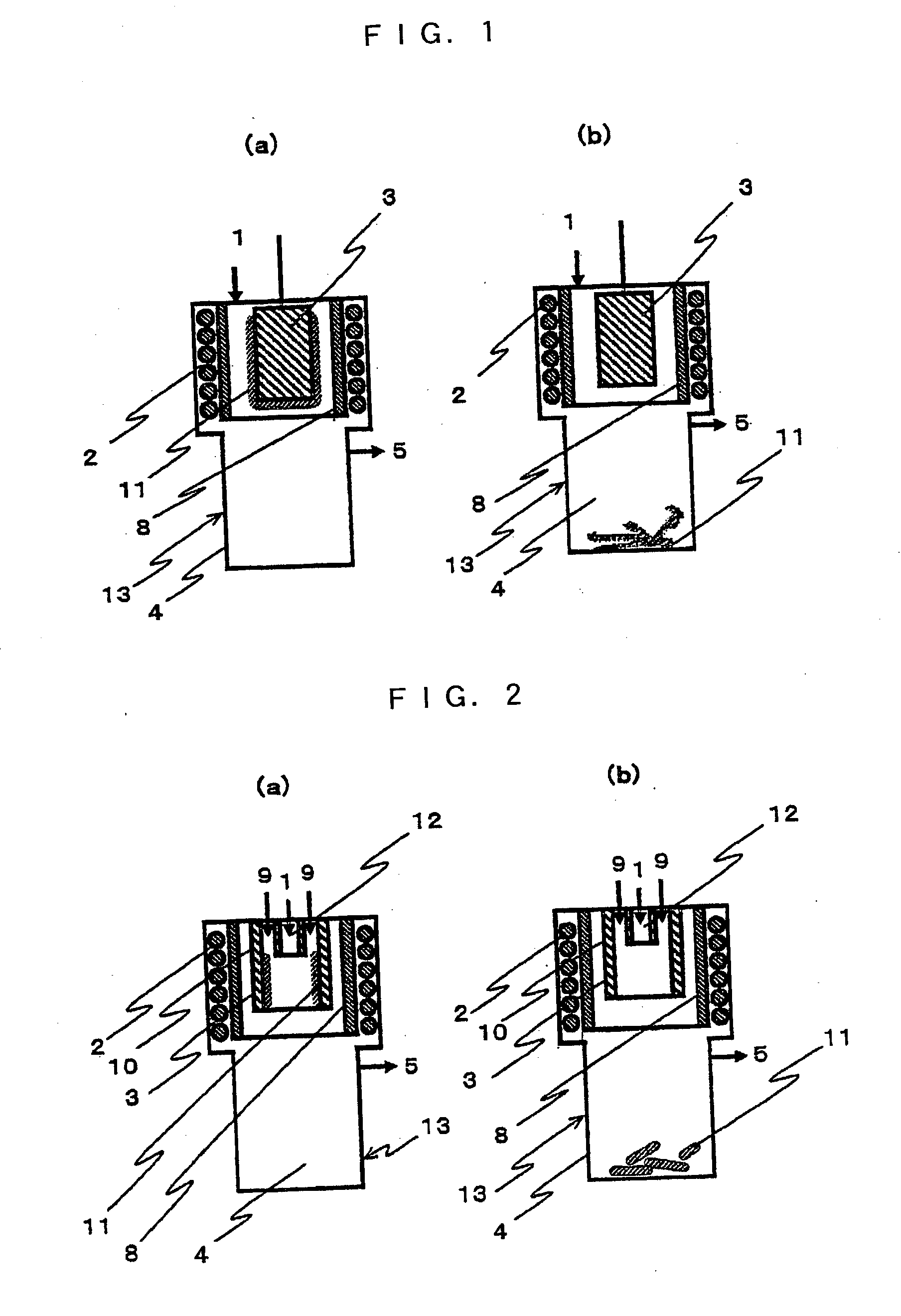
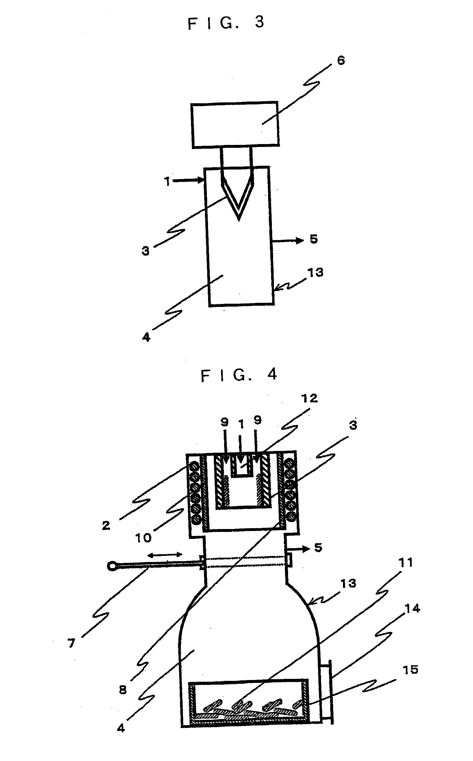
Image

Examples
example 1
[0070] A reactor having the structure shown in FIG. 4 was used. More specifically, as a substrate 3, a graphite cylinder having an internal surface coated with CVD-SiC and having an internal diameter of 50 mm, a length of 30 mm and a thickness of 1 mm was used, and around the cylinder, an electromagnetic wave generating coil having a frequency of 8 kHz was disposed as a heater 2 via a cylindrical partition wall 8 made of SIALON so that an electromagnetic wave can be applied to the graphite cylinder from the coil so as to heat the cylinder.
[0071] The graphite cylinder as the substrate 3 was heated by the above heater 2 and maintained in such a state that the temperature of its entire internal surface would be about 1,400.degree. C. Then, a mixed gas comprising hydrogen and trichlorosilane as a raw material gas was fed from a feed port 1 into the substrate 2 via a feed pipe 12 at rates of hydrogen and trichlorosilane of 100 NL / min and 60 g / min, respectively, so as to deposit silicon i...
example 2
[0077] Silicon was deposited and molten in the same manner as in Example 1 except that the internal wall of the graphite cylinder as the substrate 3 was coated with pyrocarbon.
[0078] As a result, the silicon was deposited in an amount of about 370 g per hour. Further, when all recovered deposits were formed into a single crystal and the concentration of carbon was measured by an FT-IR process, it was about 2 ppm.
example 3
[0079] Silicon was deposited and molten in the same manner as in Example 1 except that a silicon nitride cylinder molded by sintering was inserted into the graphite cylinder as the substrate 3.
[0080] As a result, the silicon was deposited in an amount of about 370 g per hour. Further, when all recovered deposits were formed into a single crystal and the concentration of carbon was measured by an FT-IR process, it was not larger than 1 ppm which was a lower detection limit.
PUM
 Abstract
Description
Claims
Application Information