Exposure method and device for forming patterns on printed wiring board

a technology of printed wiring board and pattern, which is applied in the direction of circuit masks, printers, instruments, etc., can solve the problems of increasing the quantity of drawing data to be processed, and reducing the quality of the printed imag

Inactive Publication Date: 2003-07-03
SHINKO ELECTRIC IND CO LTD
View PDF11 Cites 20 Cited by
  • Summary
  • Abstract
  • Description
  • Claims
  • Application Information

AI Technical Summary

Problems solved by technology

However, in the conventional exposure method using a set of photo masks, it is necessary to reproduce, maintain and keep the photo mask, which is expensive.
Further, when the design is changed, it is necessary to remake the mas...

Method used


Image

  • Exposure method and device for forming patterns on printed wiring board
  • Exposure method and device for forming patterns on printed wiring board
  • Exposure method and device for forming patterns on printed wiring board

Examples


Embodiment Construction

[0037] Referring to the accompanying drawings, the present invention will be explained in detail as follows.

[0038] Before the detailed explanation of the embodiment, some of the general exposure methods will be described.

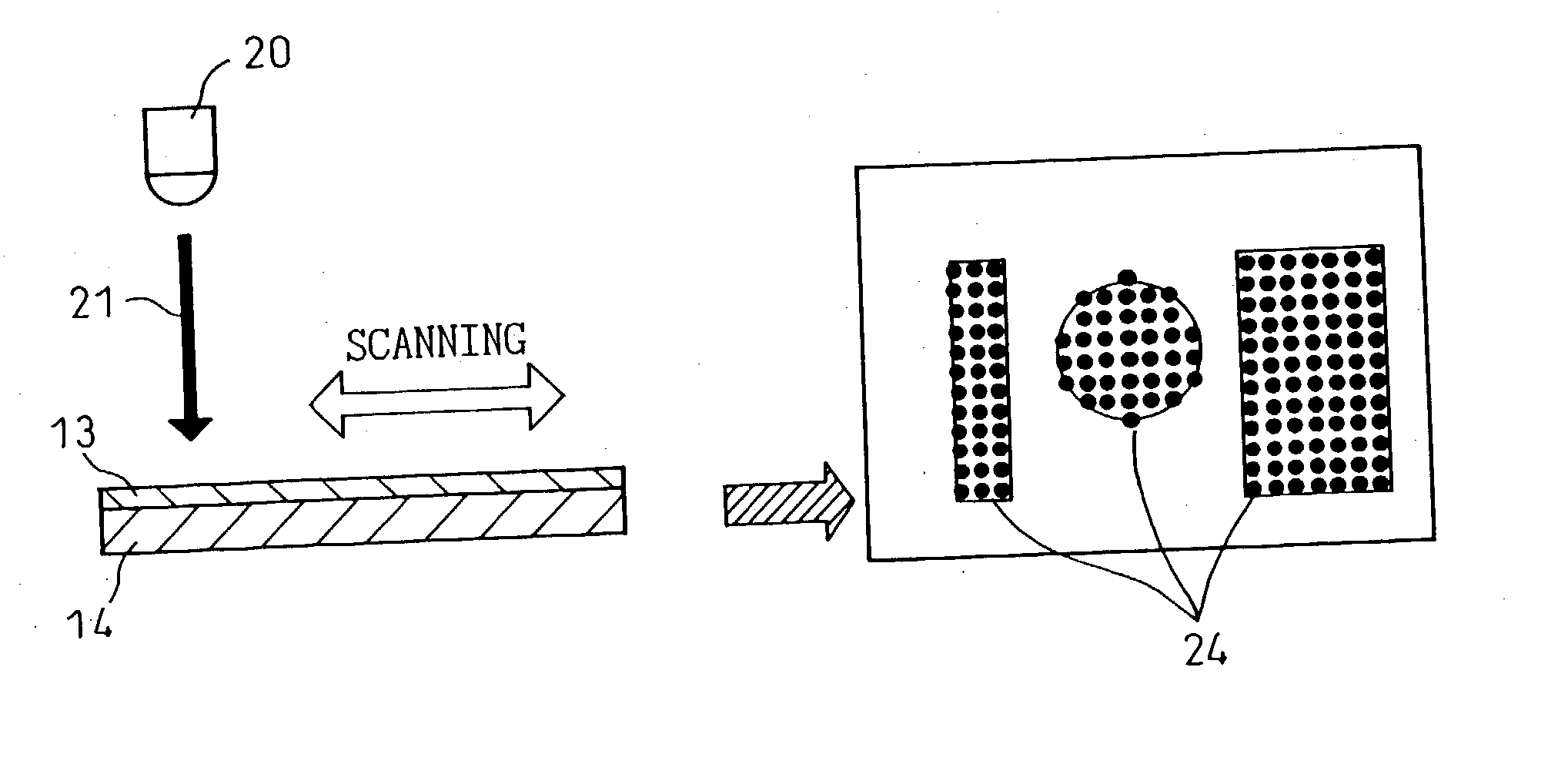
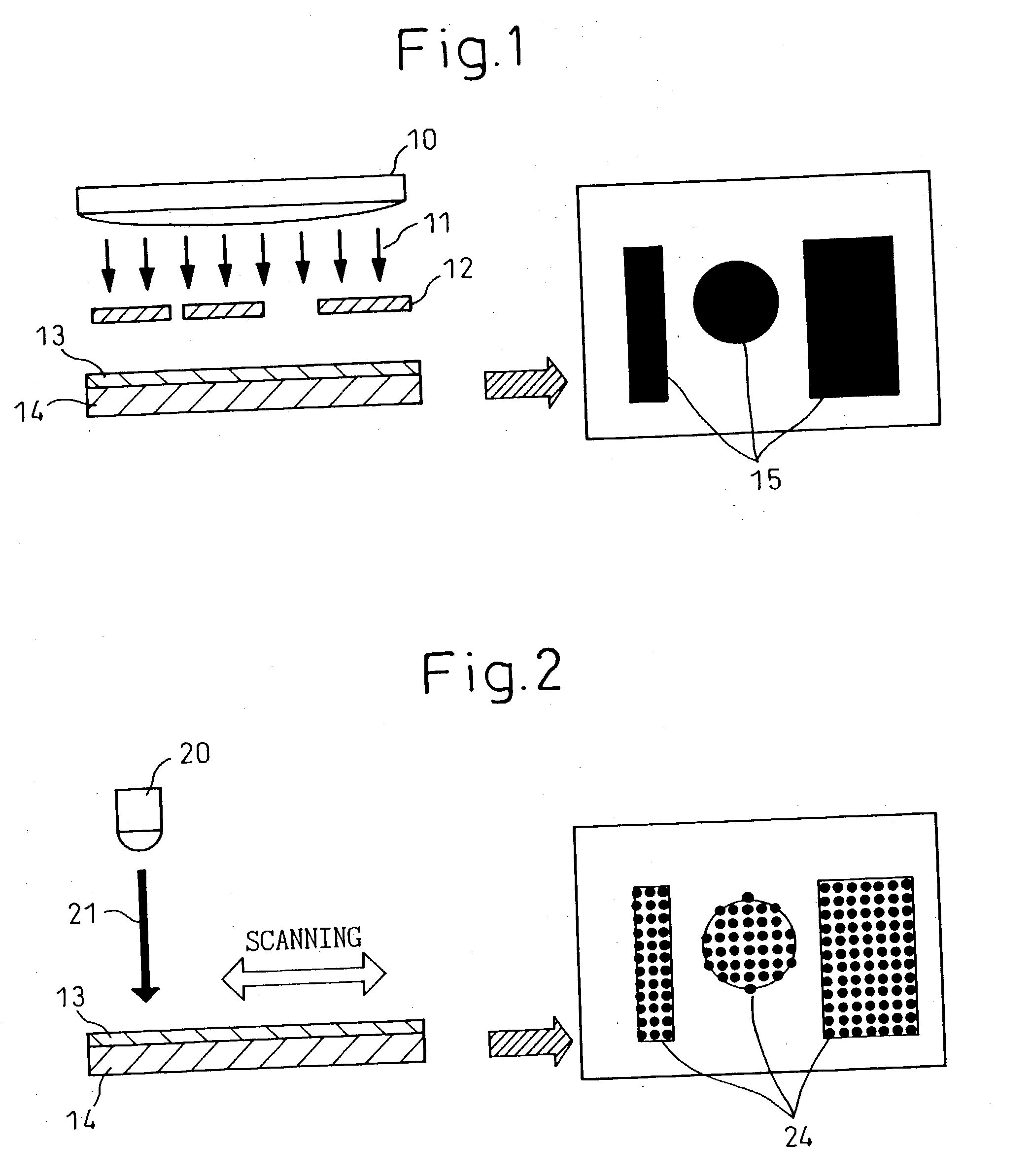
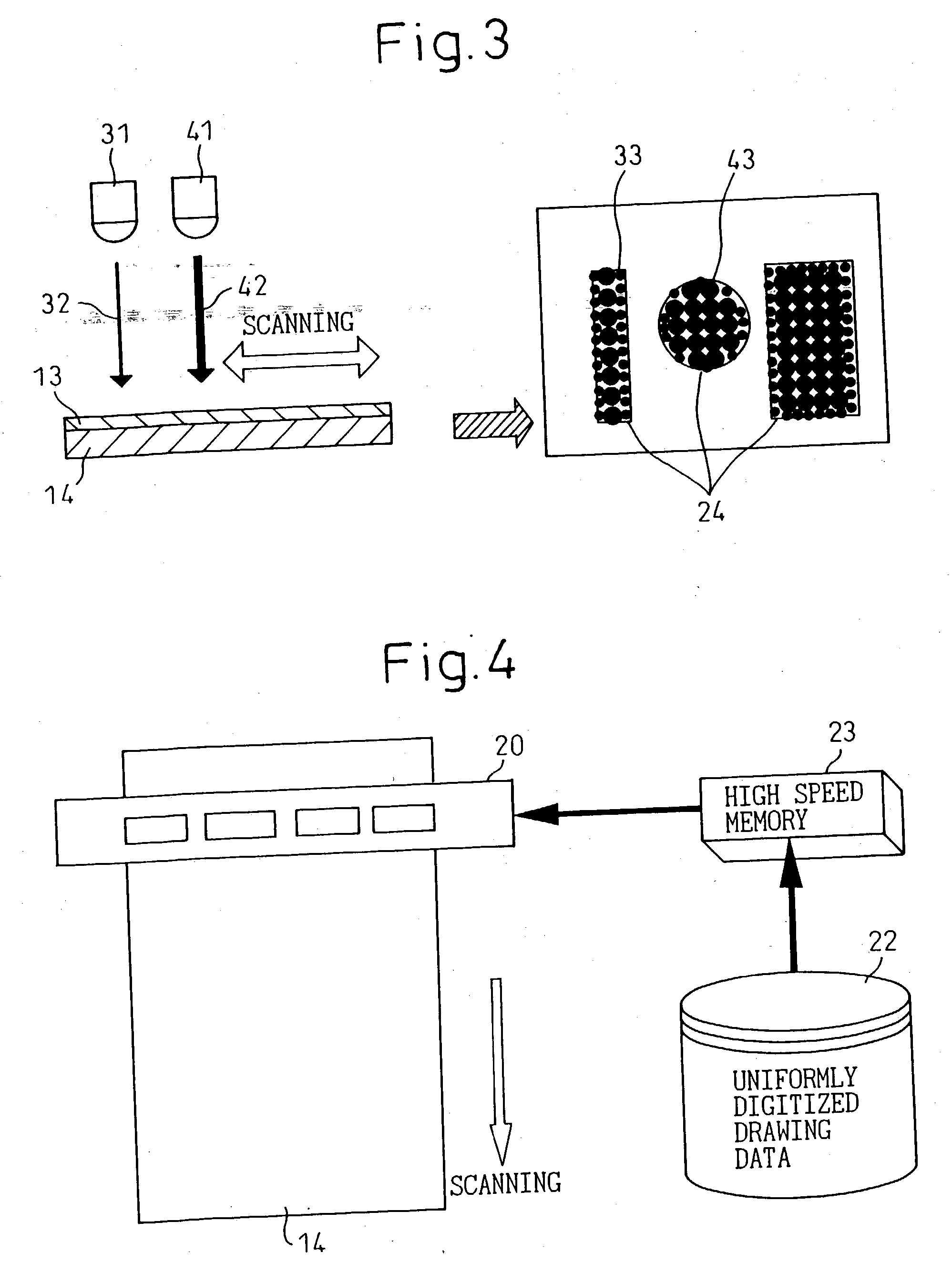
[0039] FIG. 1 is a view showing an exposure method according to the technique of photolithography in which a photo mask is used. Exposure light (11) emitted from the optical source (10) passes through the photo mask (12) and is irradiated on the substrate (14), on the surface of which resist (13) is coated. Due to the irradiation of light, the exposure portion (15) shown on the right of FIG. 1 is formed according to the pattern profile of the photo mask (12). As described above, this technique has disadvantages which are caused by using the photo mask. When the photo mask is used, it is necessary to reproduce, maintain and keep the photo mask, which is expensive. Further, when the design of the photomask is changed, it is necessary to remake the mask itself, which i...


PUM


Abstract

An optical exposure method and a device are used for forming patterns on a printed board wiring or semiconductor board. A single exposing region of a surface to be exposed is irradiated with a plurality of optical beams having different irradiating areas and different scanning speeds, such as, a peripheral area is irradiated with an optical beam having a smaller irradiating area and an inner area is irradiated with an optical beam having a larger irradiating area.

Description

[0001] 1. Field of the Invention[0002] The present invention relates to an exposure method and device. More particularly, the present invention relates to an exposure method and device for forming an exposure pattern on a printed wiring board, package or semiconductor substrate (semiconductor wafer) with a plurality of optical sources capable of irradiating light on different irradiating areas and at scanning pitches. Further, the present invention relates to a medium into which a program for executing the above exposure method is incorporated.[0003] When a printed circuit board or package is manufactured by a conventional manufacturing method, a pattern such as a wiring pattern is formed by a technique, called photolithography, using a photomask.[0004] 2. Description of the Related Art[0005] A conventional exposure method according to the photolithography technique uses a set of photo masks. Exposure light emitted from the optical source passes through the photo mask and is irradia...

Claims


Application Information

Patent Timeline
IPC IPC(8): G03F7/20H01L21/027H05K3/00
CPCG03F7/70283H05K3/0082G03F7/70466G03F7/70291
Inventor SEKIGAWA, KAZUNARIAKAGAWA, MASATOSHI
Owner SHINKO ELECTRIC IND CO LTD
Why Eureka
Try Eureka