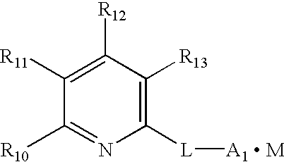
Charge transfer material, and photoelectric conversion device and photoelectric cell using same, and pyridine compound
a charge transfer material and charge transfer layer technology, applied in the direction of non-metal conductors, electrochemical generators, electrolytic capacitors, etc., can solve the problems of drastic decrease in charge transportability, disadvantageous durability of long-term operation and insufficient photoelectric conversion efficiency of photoelectric conversion devices comprising this charge transfer material as a charge transfer layer. , to achieve the effect of excellent charge transportability and durability
- Summary
- Abstract
- Description
- Claims
- Application Information
AI Technical Summary
Benefits of technology
Problems solved by technology
Method used
Image
Examples
example 2
[0181] 1. Preparation of Titanium Dioxide Dispersion
[0182] A dispersion of titanium dioxide particles, whose concentration was 11% by mass, was prepared in the same manner as in the method described in Christophe J. Barb'e, et al, the Journal of American Ceramic Society, Vol. 80, No. 12, page 3157 (1997) except that an autoclave temperature was 230.degree. C. The average particle diameter of the titanium dioxide particles in the dispersion was about 10 nm. Added to and mixed with this dispersion was polyethylene glycol (molecular weight: 20000, available from Wako Pure Chemical Industries, Ltd) in an amount of 20% by mass based on the titanium dioxide, to obtain a dispersion of titanium dioxide particles.
[0183] 2. Preparation of Dye-Adsorbed Titanium Dioxide Electrode
[0184] (1) Preparation of Dye-Adsorbed Electrode
[0185] The above dispersion of titanium dioxide particles was applied to an electrically conductive, transparent glass coated with fluorine-doped tin oxide (surface resist...
example 3
[0204] Dye-adsorbed electrodes T-2 to T-4 were produced in the same manner as in the dye-adsorbed electrode T-1 except that ruthenium complex dye R-10, merocyanine dye M-3 or squarylium dye M-1 was used in place of the ruthenium complex dye R-1. The concentration of the dye in the dye adsorption liquid was 1.times.10.sup.-4 mol / L. With the dye-adsorbed electrodes T-2 to T-4 and the charge transfer materials shown in Table 4, comparative photoelectric conversion devices C-27, C-28, C-30, C-31, C-33 and C-34 and photoelectric conversion devices C-29, C-32 and C-35 of the present invention were produced in the same manner as in Example 2. The photoelectric conversion efficiency and durability of each photoelectric conversion device were evaluated in the same manner as in Example 2, providing the same results as in Example 2, as shown in Table 4.
7 TABLE 4 Photoelectric Conversion Efficiency (%) Photoelectric Charge After Conversion Transfer 3-month Device Electrode Dye Material Initial ...
PUM
| Property | Measurement | Unit |
|---|---|---|
| Electrical conductance | aaaaa | aaaaa |
| Electrical conductance | aaaaa | aaaaa |
| Electrical conductance | aaaaa | aaaaa |
Abstract
Description
Claims
Application Information


