Exchange coupling film, magneto-resistance effect device, magnetic head, and magnetic random access memory

a technology of exchange coupling and magnetoresistance, which is applied in the direction of nanoinformatics, magnetic bodies, instruments, etc., can solve the problems of insufficient separation of free layer and pinning layer hysteresis, inability to realize good device operation, and insufficient coercive force of pinning layer

Inactive Publication Date: 2003-07-10
NEC CORP
View PDF7 Cites 125 Cited by
  • Summary
  • Abstract
  • Description
  • Claims
  • Application Information

AI Technical Summary

Problems solved by technology

However there is a problem that the coercive force of the pinning layer is large and an area where the magnetic moment of the free layer is antiparallel to the magnetic moment of the pinning layer is narrow, a technique which reduces the coercive force of the pinning layer by inserting the interface control layer made of the nonmagnetic metal or the oxide material including Cr or Mn with the film thickness of 0.3 to 2 nm between the antiferromagnetic layer of NiO and the pinning layer (ferromagnetic layer) is described in Japanese Patent No. 2850866.
Especially, in the exchange coupling film made of the antiferromagnetic layer of the ordered alloy, though the exchange coupling magnetic field is relatively large, the coercive force of the pinning layer becomes considerably large, which causes the hysteresis of the free layer and the hysteresis of the pinning layer to be separated insufficiently in case of the spin valve type of magneto-resistance effect device.
As a result, there is a problem that good device operation can not be realized.
Accordingly, it is found that the relatively large exchange coupling magnetic field and the small coercive force of the pinning layer can be compatible by the multilayered pinning layer, however it is difficult to achieve in the single pinning layer.
The first problem is that sufficiently large antiferromagnetic coupling needs to act between two magnetic material layers, so that the film thickness of the spacer layer requires strict control.
The second problem is that, as described in Japanese Patent Application Laid-Open No. 2000-315305, it is necessary to form the pinning layer by the AFC film and another ferromagnetic layer in order to reduce the coercive force of the AFC film, which results in increment of the number of necessary targets forming the AFC film and enlargement of a manufacturing apparatus.
However, in the technique disclosed in Japanese Patent Application Laid-Open No. 232617 / 1999, the second ferromagnetic layer (pinning layer) is consisted of at least two ferromagnetic layers, one of the two layers uses the ferromagnetic layer obtaining the large exchange coupling energy, and the other layer uses the ferromagnetic layer having the small saturation magnetization, when at least two ferromagnetic layers are deposited, the obtained characteristics as a whole become average characteristics of each layer, which causes remarkable performance not to be obtained.
However, there are problems described below in the above described conventional techniques.
It is difficult that the larger exchange coupling magnetic field and the smaller coercive force of the pinning layer are simultaneously achieved even in the exchange coupling film using the antiferromagnetic layer as described above.
In the method that the ferromagnetic layer of the pinning layer is formed by at least two ferromagnetic layers, when the antiferromagnetic layer is made of the antiferromagnetic material including the ordered alloy of the L1.sub.0 type (CuAu--I type) of face-centered cubic structure such as a PtMn alloy, a PdMn alloy, and a NiMn alloy, there is a problem which effect of the double-layered film is small, because it is not possible to reduce the coercive force of the pinning layer by the multilayered film of the pinning layer even though the exchange coupling energy can be increased somewhat compared with the single layer film of the pinning layer.
As described above, sufficient performance of the spin valve type of magneto-resistance effect device can not be obtained in any conventional techniques.

Method used


Image

  • Exchange coupling film, magneto-resistance effect device, magnetic head, and magnetic random access memory
  • Exchange coupling film, magneto-resistance effect device, magnetic head, and magnetic random access memory
  • Exchange coupling film, magneto-resistance effect device, magnetic head, and magnetic random access memory

Examples


second experiment

[0102] (Second Experiment)

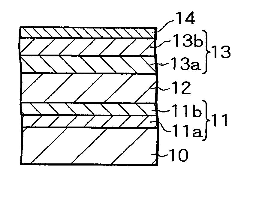
[0103] A second experiment will be described. The exchange coupling film of the second experiment is the exchange coupling film having the Top-AF type of configuration shown in FIG. 3. The exchange coupling film having the double-layered pinning layer whose pinning layer 13 includes the exchange coupling giving layer 13a and the exchange coupling enhancement layer 13b of the invention was produced as the experiment, the exchange coupling film having the conventional single-layered pinning layer was also produced for comparison. Concretely, a Ta layer (1.5 nm) as the foundation layer 11a, a NiFe layer (2.0 nm) as the foundation layer 11b, the single or double-layered antiferromagnetic layer shown below as the pinning layer 13, an IrMn layer (10 nm) as the antiferromagnetic layer 12, and a Ta layer (3.0 nm) as the cap protection layer 14 were formed on the silicon substrate 10 whose surface was thermal-oxidized in the order. The pinning layers 13 were prepare...

third experiment

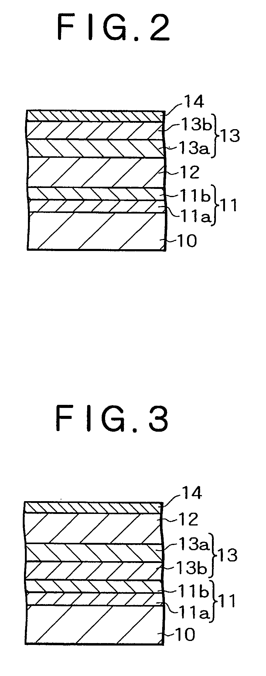
[0105] (Third Experiment)

[0106] A third experiment will be explained. It is a purpose of the third experiment to study an effect which a combination of the exchange coupling giving layer and the exchange coupling enhancement layer affects the exchange coupling. The exchange coupling film of the third experiment is the Bottom-AF type of exchange coupling film shown in FIG. 2. A Ta layer (5 nm) as the foundation layer 11a, a Cu layer (3 nm) as the foundation layer 11b, an IrMn layer (10 nm) as the antiferromagnetic layer 12, a ferromagnetic layer of combinations shown below as the exchange coupling giving layer 13a and the exchange coupling enhancement layer 13b, and a Ta layer (5 nm) as the cap protection layer 14 were formed on the silicon substrate 10 whose surface was thermal-oxidized in the order to produce the exchange coupling film of the double layered pinning layer. The combination of exchange coupling giving layer 13a / exchange coupling enhancement layer 13b were prepared as ...

fourth experiment

[0110] (Fourth Experiment)

[0111] As described above, in order to increase the exchange coupling in the double-layered pinning layer, it was found that the combination of the exchange coupling giving layer and the exchange coupling enhancement layer is important and NiFe is not preferable to the exchange coupling giving layer and the exchange coupling enhancement layer. In the fourth experiment, a combination in which the large exchange coupling can be obtained by a CoFe alloy was studied.

[0112] The exchange coupling film of the fourth experiment is the exchange coupling film having the Bottom-AF type of configuration shown in FIG. 2. A Ta layer (5 nm) as the foundation layer 11a, a Cu layer (3 nm) as the foundation layer 11b, an IrMn layer (10 nm) as the antiferromagnetic layer 12, a ferromagnetic layer of combinations shown below as the exchange coupling giving layer 13a and the exchange coupling enhancement layer 13b, and a Ta layer (5 nm) as the cap protection layer 14 were forme...


PUM


Abstract

A foundation layer increasing adhesive properties to a substrate, another foundation layer controlling orientation of an antiferromagnetic layer, the antiferromagnetic layer including a disordered alloy of IrMn, a pinning layer, and a cap protection layer are formed in the order on the substrate. The pinning layer includes two layers having an exchange coupling giving layer which exchange-couples to the antiferromagnetic layer and an exchange coupling enhancement layer which enhances the exchange coupling, the exchange coupling giving layer is made of a ferromagnetic material including Co or a Co100-XFeX alloy (O<=X<25) having face-centered cubic structure. The exchange coupling enhancement layer is made of Fe or a Co100-YFeY alloy (25<=Y<=100) having body-centered cubic structure.

Description

[0001] 1. Field of the Invention[0002] The present invention relates to an exchange coupling film utilizing exchange coupling which acts between a ferromagnetic layer and an antiferromagnetic layer, a magneto-resistance effect device having the exchange coupling film, and a reproducing magnetic head and a magnetic random access memory which use the magneto-resistance effect device.[0003] 2. Description of the Related Art[0004] A so-called spin valve type of magneto-resistance effect device is used for a magnetic random access memory (MRAM) which is notable as a reproducing magnetic head and a nonvolatile memory of a hard disk drive (HDD) apparatus corresponding to high magnetic recording density. A basic structure of the spin valve type of magneto-resistance effect device is a multilayer in which a ferromagnetic layer, a nonmagnetic material layer, the ferromagnetic layer, and an antiferromagnetic layer are formed in the order or in reverse. At this point, a magnetic moment of the f...

Claims


Application Information

Patent Timeline
Patent Type & Authority Applications(United States)
IPC IPC(8): G01R33/09G11B5/39G11C11/15H01F10/16H01F10/187H01F10/32H01L21/8246H01L27/105H01L27/22H01L43/08
CPCB82Y10/00B82Y25/00G01R33/093G11B5/3932H01L43/08G11C11/15H01F10/3268H01L27/222G11B2005/3996H10B61/00H10N50/10
Inventor KAMIJO, ATSUSHI
Owner NEC CORP
Why Eureka
Try Eureka